- 您现在的位置:买卖IC网 > PDF目录10967 > MCHC908JW32FAE (Freescale Semiconductor)IC MCU 32K FLASH 8MHZ 48-LQFP PDF资料下载
参数资料
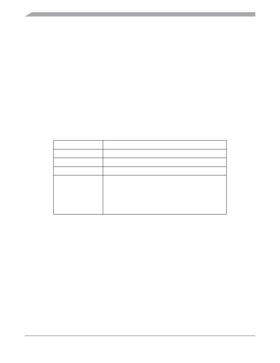
| 型号: | MCHC908JW32FAE |
| 厂商: | Freescale Semiconductor |
| 文件页数: | 7/232页 |
| 文件大小: | 0K |
| 描述: | IC MCU 32K FLASH 8MHZ 48-LQFP |
| 标准包装: | 250 |
| 系列: | HC08 |
| 核心处理器: | HC08 |
| 芯体尺寸: | 8-位 |
| 速度: | 8MHz |
| 连通性: | SPI,USB |
| 外围设备: | LED,LVD,POR,PWM |
| 输入/输出数: | 29 |
| 程序存储器容量: | 32KB(32K x 8) |
| 程序存储器类型: | 闪存 |
| RAM 容量: | 1K x 8 |
| 电压 - 电源 (Vcc/Vdd): | 3.5 V ~ 5.5 V |
| 振荡器型: | 内部 |
| 工作温度: | 0°C ~ 70°C |
| 封装/外壳: | 48-LQFP |
| 包装: | 托盘 |
第1页第2页第3页第4页第5页第6页当前第7页第8页第9页第10页第11页第12页第13页第14页第15页第16页第17页第18页第19页第20页第21页第22页第23页第24页第25页第26页第27页第28页第29页第30页第31页第32页第33页第34页第35页第36页第37页第38页第39页第40页第41页第42页第43页第44页第45页第46页第47页第48页第49页第50页第51页第52页第53页第54页第55页第56页第57页第58页第59页第60页第61页第62页第63页第64页第65页第66页第67页第68页第69页第70页第71页第72页第73页第74页第75页第76页第77页第78页第79页第80页第81页第82页第83页第84页第85页第86页第87页第88页第89页第90页第91页第92页第93页第94页第95页第96页第97页第98页第99页第100页第101页第102页第103页第104页第105页第106页第107页第108页第109页第110页第111页第112页第113页第114页第115页第116页第117页第118页第119页第120页第121页第122页第123页第124页第125页第126页第127页第128页第129页第130页第131页第132页第133页第134页第135页第136页第137页第138页第139页第140页第141页第142页第143页第144页第145页第146页第147页第148页第149页第150页第151页第152页第153页第154页第155页第156页第157页第158页第159页第160页第161页第162页第163页第164页第165页第166页第167页第168页第169页第170页第171页第172页第173页第174页第175页第176页第177页第178页第179页第180页第181页第182页第183页第184页第185页第186页第187页第188页第189页第190页第191页第192页第193页第194页第195页第196页第197页第198页第199页第200页第201页第202页第203页第204页第205页第206页第207页第208页第209页第210页第211页第212页第213页第214页第215页第216页第217页第218页第219页第220页第221页第222页第223页第224页第225页第226页第227页第228页第229页第230页第231页第232页
Monitor Mode (MON)
MC68HC908JW32 Data Sheet, Rev. 6
104
Freescale Semiconductor
The control and data bytes are described below.
Bus speed — This one byte indicates the operating bus speed of the MCU. The value of this byte
should be equal to 4 times the bus speed. E.g. for a 4MHz bus, the value is 16 ($10). This control
byte is useful where the MCU clock source is switched between the PLL clock and the crystal clock.
Data size — This one byte indicates the number of bytes in the data array that are to be
manipulated. The maximum data array size is 255. Routines ERARNGE and MON_ERARNGE do
not manipulate a data array, thus, this data size byte has no meaning.
Start address — These two bytes, high byte followed by low byte, indicate the start address of the
FLASH memory to be manipulated.
Data array — This data array contains data that are to be manipulated. Data in this array are
programmed to FLASH memory by the programming routines: PRGRNGE, MON_PRGRNGE. For
the read routines: LDRNGE and data is read from FLASH and stored in this array.
7.5.1 PRGRNGE
PRGRNGE is used to program a range of FLASH locations with data loaded into the data array.
The start location of the FLASH to be programmed is specified by the address ADDRH:ADDRL and the
number of bytes from this location is specified by DATASIZE. The maximum number of bytes that can be
programmed in one routine call is 255 bytes (max. DATASIZE is 255).
ADDRH:ADDRL do not need to be at a page boundary, the routine handles any boundary misalignment
during programming. A check to see that all bytes in the specified range are erased is not performed by
this routine prior programming. Nor does this routine do a verification after programming, so there is no
return confirmation that programming was successful. User must assure that the range specified is first
erased.
The coding example below is to program 64 bytes of data starting at FLASH location $EE00, with a bus
speed of 4.9152 MHz. The coding assumes the data block is already loaded in RAM, with the address
pointer, FILE_PTR, pointing to the first byte of the data block.
Table 7-11. PRGRNGE Routine
Routine Name
PRGRNGE
Routine Description
Program a range of locations
Calling Address
$FE10
Stack Used
16 bytes
Data Block Format
Bus speed (BUS_SPD)
Data size (DATASIZE)
Start address high (ADDRH)
Start address (ADDRL)
Data 1 (DATA1)
:
Data N (DATAN)
相关PDF资料 |
PDF描述 |
|---|---|
| S9S08DZ128F2MLL | MCU 128K FLASH AUTO 100-LQFP |
| MC9S08DV32CLF | IC MCU 32K FLASH 2K RAM 48-LQFP |
| IDTNW6005AS | IC CALLER ID DECODER 20-SOIC |
| HR25A-7R-6PA | CONN RCPT 6POS MALE SLD PCB |
| VI-B1B-IY-F3 | CONVERTER MOD DC/DC 95V 50W |
相关代理商/技术参数 |
参数描述 |
|---|---|
| MCHC908JW32FC | 功能描述:8位微控制器 -MCU MCHC908JW32FC RoHS:否 制造商:Silicon Labs 核心:8051 处理器系列:C8051F39x 数据总线宽度:8 bit 最大时钟频率:50 MHz 程序存储器大小:16 KB 数据 RAM 大小:1 KB 片上 ADC:Yes 工作电源电压:1.8 V to 3.6 V 工作温度范围:- 40 C to + 105 C 封装 / 箱体:QFN-20 安装风格:SMD/SMT |
| MCHC908JW32FCR | 制造商:Freescale Semiconductor 功能描述:8-BIT HC08 CISC 32KB FLASH 5V 48-PIN QFN EP T/R - Tape and Reel |
| MCHC908JW32FHE | 制造商:Rochester Electronics LLC 功能描述: 制造商:Freescale Semiconductor 功能描述: |
| MCHC908LK24CFQE | 功能描述:8位微控制器 -MCU 8 BIT MCU RoHS:否 制造商:Silicon Labs 核心:8051 处理器系列:C8051F39x 数据总线宽度:8 bit 最大时钟频率:50 MHz 程序存储器大小:16 KB 数据 RAM 大小:1 KB 片上 ADC:Yes 工作电源电压:1.8 V to 3.6 V 工作温度范围:- 40 C to + 105 C 封装 / 箱体:QFN-20 安装风格:SMD/SMT |
| MCHC908MR8CFAE | 功能描述:8位微控制器 -MCU 8 BIT MCU RoHS:否 制造商:Silicon Labs 核心:8051 处理器系列:C8051F39x 数据总线宽度:8 bit 最大时钟频率:50 MHz 程序存储器大小:16 KB 数据 RAM 大小:1 KB 片上 ADC:Yes 工作电源电压:1.8 V to 3.6 V 工作温度范围:- 40 C to + 105 C 封装 / 箱体:QFN-20 安装风格:SMD/SMT |
发布紧急采购,3分钟左右您将得到回复。