- 您现在的位置:买卖IC网 > PDF目录10932 > MCIMX31CJMN4DR2 (Freescale Semiconductor)MPU MX31 ARM11 473-MAPBGA PDF资料下载
参数资料
| 型号: | MCIMX31CJMN4DR2 |
| 厂商: | Freescale Semiconductor |
| 文件页数: | 17/108页 |
| 文件大小: | 0K |
| 描述: | MPU MX31 ARM11 473-MAPBGA |
| 标准包装: | 750 |
| 系列: | i.MX31 |
| 核心处理器: | ARM11 |
| 芯体尺寸: | 32-位 |
| 速度: | 400MHz |
| 连通性: | 1 线,EBI/EMI,I²C,MMC,SPI,SSI,UART/USART,USB OTG |
| 外围设备: | DMA,LCD,POR,PWM,WDT |
| 输入/输出数: | 32 |
| 程序存储器类型: | ROMless |
| RAM 容量: | 16K x 8 |
| 电压 - 电源 (Vcc/Vdd): | 1.22 V ~ 1.65 V |
| 振荡器型: | 外部 |
| 工作温度: | -40°C ~ 85°C |
| 封装/外壳: | 473-LFBGA |
| 包装: | 带卷 (TR) |
第1页第2页第3页第4页第5页第6页第7页第8页第9页第10页第11页第12页第13页第14页第15页第16页当前第17页第18页第19页第20页第21页第22页第23页第24页第25页第26页第27页第28页第29页第30页第31页第32页第33页第34页第35页第36页第37页第38页第39页第40页第41页第42页第43页第44页第45页第46页第47页第48页第49页第50页第51页第52页第53页第54页第55页第56页第57页第58页第59页第60页第61页第62页第63页第64页第65页第66页第67页第68页第69页第70页第71页第72页第73页第74页第75页第76页第77页第78页第79页第80页第81页第82页第83页第84页第85页第86页第87页第88页第89页第90页第91页第92页第93页第94页第95页第96页第97页第98页第99页第100页第101页第102页第103页第104页第105页第106页第107页第108页
MCIMX31C/MCIMX31LC Technical Data, Rev. 4.3
16
Freescale Semiconductor
Electrical Characteristics
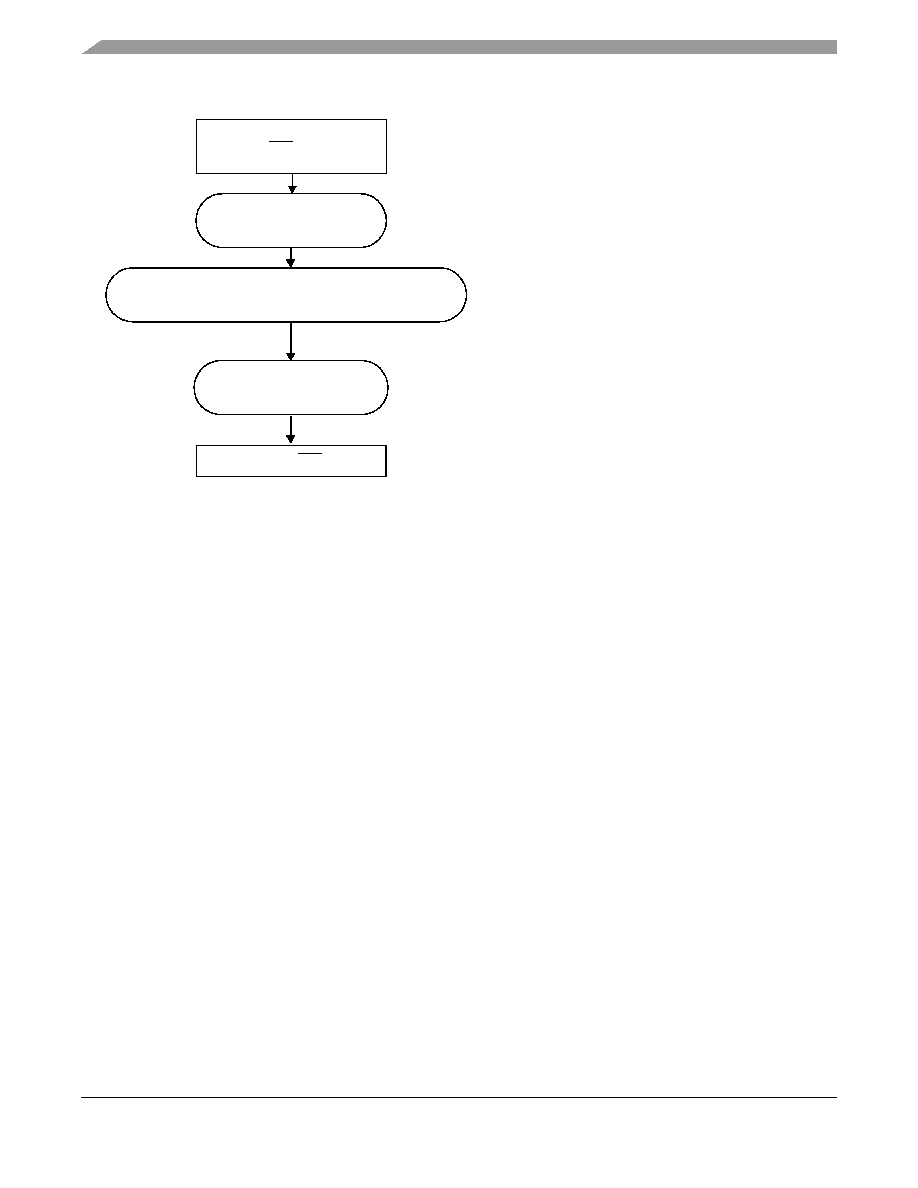
Figure 3. Option 2 Power-Up Sequence (Silicon Revision 2.0 and 2.0.1)
4.2.2
Powering Down
The power-down sequence should be completed as follows:
1. Lower the FUSE_VDD supply (when in write mode).
2. Lower the remaining supplies.
4.3
Module-Level Electrical Specifications
This section contains the MCIMX31C electrical information including timing specifications, arranged in
alphabetical order by module name.
4.3.1
I/O Pad (PADIO) Electrical Specifications
This section specifies the AC/DC characterization of functional I/O of the MCIMX31C. There are two
main types of I/O: regular and DDR. In this document, the “Regular” type is referred to as GPIO.
4.3.1.1
DC Electrical Characteristics
The MCIMX31C I/O parameters appear in Table 12 for GPIO. See Table 7, "Operating Ranges," on page
12 for temperature and supply voltage ranges.
Release POR
QVCC, QVCC1, QVCC4
IOQVDD, NVCC1, NVCC3–10, NVCC2, NVCC21, NVCC22
Hold POR Asserted
Notes:
1
The board design must guarantee that supplies reach
90% level before transition to the next state, using Power
Management IC or other means.
2
The NVCC1 supply must not precede IOQVDD by more
than 0.2 V until IOQVDD has reached 1.5 V. If IOQVDD
is powered up first, there are no restrictions.
3
Raising NVCC2, NVCC21, and NVCC22 at the same
time as IOQVDD does not produce the slight increase in
current drain on IOQVDD (as described in Figure 2,
Note 5).
4
FUSE_VDD should not be driven on power-up for Silicon
Revision2.0 and 2.0.1. This supply is dedicated for fuse
burning (programming), and should not be driven upon
boot-up.
FVCC, MVCC, SVCC, UVCC
4
相关PDF资料 |
PDF描述 |
|---|---|
| VE-2NB-CU | CONVERTER MOD DC/DC 95V 200W |
| MCIMX31CJMN4CR2 | MPU MX31 ARM11 473-MAPBGA |
| MCIMX31CJMN4C | MPU MX31 ARM11 473-MAPBGA |
| MCIMX31CVMN4C | IC MPU MAP I.MX31 473-MAPBGA |
| MCIMX31CVMN4CR2 | IC MPU MAP I.MX31 473-MAPBGA |
相关代理商/技术参数 |
参数描述 |
|---|---|
| MCIMX31CVKN5C | 功能描述:IC MPU MAP I.MX31 457-MAPBGA RoHS:是 类别:集成电路 (IC) >> 嵌入式 - 微控制器, 系列:i.MX31 标准包装:1 系列:AVR® ATmega 核心处理器:AVR 芯体尺寸:8-位 速度:16MHz 连通性:I²C,SPI,UART/USART 外围设备:欠压检测/复位,POR,PWM,WDT 输入/输出数:32 程序存储器容量:32KB(16K x 16) 程序存储器类型:闪存 EEPROM 大小:1K x 8 RAM 容量:2K x 8 电压 - 电源 (Vcc/Vdd):2.7 V ~ 5.5 V 数据转换器:A/D 8x10b 振荡器型:内部 工作温度:-40°C ~ 125°C 封装/外壳:44-TQFP 包装:剪切带 (CT) 其它名称:ATMEGA324P-B15AZCT |
| MCIMX31CVKN5C | 制造商:Freescale Semiconductor 功能描述:Microcontroller |
| MCIMX31CVKN5CR2 | 功能描述:IC MPU MAP I.MX31 457-MAPBGA RoHS:是 类别:集成电路 (IC) >> 嵌入式 - 微控制器, 系列:i.MX31 标准包装:1 系列:AVR® ATmega 核心处理器:AVR 芯体尺寸:8-位 速度:16MHz 连通性:I²C,SPI,UART/USART 外围设备:欠压检测/复位,POR,PWM,WDT 输入/输出数:32 程序存储器容量:32KB(16K x 16) 程序存储器类型:闪存 EEPROM 大小:1K x 8 RAM 容量:2K x 8 电压 - 电源 (Vcc/Vdd):2.7 V ~ 5.5 V 数据转换器:A/D 8x10b 振荡器型:内部 工作温度:-40°C ~ 125°C 封装/外壳:44-TQFP 包装:剪切带 (CT) 其它名称:ATMEGA324P-B15AZCT |
| MCIMX31CVKN5D | 功能描述:处理器 - 专门应用 2.0.1 CONSUMER FULL RoHS:否 制造商:Freescale Semiconductor 类型:Multimedia Applications 核心:ARM Cortex A9 处理器系列:i.MX6 数据总线宽度:32 bit 最大时钟频率:1 GHz 指令/数据缓存: 数据 RAM 大小:128 KB 数据 ROM 大小: 工作电源电压: 最大工作温度:+ 95 C 安装风格:SMD/SMT 封装 / 箱体:MAPBGA-432 |
| MCIMX31CVKN5DR2 | 功能描述:处理器 - 专门应用 2.0.1 CONSUMER FULL RoHS:否 制造商:Freescale Semiconductor 类型:Multimedia Applications 核心:ARM Cortex A9 处理器系列:i.MX6 数据总线宽度:32 bit 最大时钟频率:1 GHz 指令/数据缓存: 数据 RAM 大小:128 KB 数据 ROM 大小: 工作电源电压: 最大工作温度:+ 95 C 安装风格:SMD/SMT 封装 / 箱体:MAPBGA-432 |
发布紧急采购,3分钟左右您将得到回复。