- 您现在的位置:买卖IC网 > PDF目录10936 > MCIMX31DVKN5D (Freescale Semiconductor)IC MPU I.MX31 CONSUMR 457TMAP PDF资料下载
参数资料
| 型号: | MCIMX31DVKN5D |
| 厂商: | Freescale Semiconductor |
| 文件页数: | 35/118页 |
| 文件大小: | 0K |
| 描述: | IC MPU I.MX31 CONSUMR 457TMAP |
| 标准包装: | 152 |
| 系列: | i.MX31 |
| 核心处理器: | ARM11 |
| 芯体尺寸: | 32-位 |
| 速度: | 532MHz |
| 连通性: | 1 线,ATA,EBI/EMI,FIR,I²C,MMC/SD,PCMCIA,SIM,SPI,SSI,UART/USART,USB,USB OTG |
| 外围设备: | DMA,LCD,POR,PWM,WDT |
| 程序存储器类型: | ROMless |
| RAM 容量: | 16K x 8 |
| 电压 - 电源 (Vcc/Vdd): | 1.22 V ~ 3.3 V |
| 振荡器型: | 外部 |
| 工作温度: | 0°C ~ 70°C |
| 封装/外壳: | 457-LFBGA |
| 包装: | 托盘 |
第1页第2页第3页第4页第5页第6页第7页第8页第9页第10页第11页第12页第13页第14页第15页第16页第17页第18页第19页第20页第21页第22页第23页第24页第25页第26页第27页第28页第29页第30页第31页第32页第33页第34页当前第35页第36页第37页第38页第39页第40页第41页第42页第43页第44页第45页第46页第47页第48页第49页第50页第51页第52页第53页第54页第55页第56页第57页第58页第59页第60页第61页第62页第63页第64页第65页第66页第67页第68页第69页第70页第71页第72页第73页第74页第75页第76页第77页第78页第79页第80页第81页第82页第83页第84页第85页第86页第87页第88页第89页第90页第91页第92页第93页第94页第95页第96页第97页第98页第99页第100页第101页第102页第103页第104页第105页第106页第107页第108页第109页第110页第111页第112页第113页第114页第115页第116页第117页第118页
Electrical Characteristics
MCIMX31/MCIMX31L Technical Data, Rev. 4.3
Freescale Semiconductor
23
4.3.3
Clock Amplifier Module (CAMP) Electrical Characteristics
This section outlines the Clock Amplifier Module (CAMP) specific electrical characteristics. Table 19
shows clock amplifier electrical characteristics.
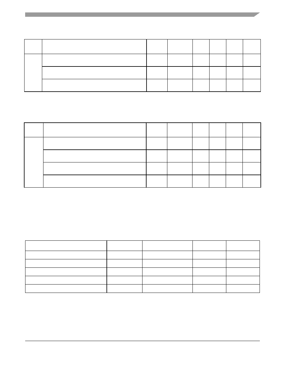
Table 17. AC Electrical Characteristics of Fast1 General I/O 2
1 Fast/slow characteristic is selected per GPIO (where available) by “slew rate” control. See reference manual.
2 Use of GPIO in fast mode with the associated NVCC > 1.95 V can result in excessive overshoot and ringing.
ID
Parameter
Symbol
Test
Condition
Min
Typ
Max
Units
PA1
Output Transition Times (Max Drive)
tpr
25 pF
50 pF
0.68
1.34
1.33
2.6
2.07
4.06
ns
Output Transition Times (High Drive)
tpr
25 pF
50 pF
.91
1.79
1.77
3.47
2.74
5.41
ns
Output Transition Times (Std Drive)
tpr
25 pF
50 pF
1.36
2.68
2.64
5.19
4.12
8.11
ns
Table 18. AC Electrical Characteristics of DDR I/O
ID
Parameter
Symbol
Test
Condition
Min
Typ
Max
Units
PA1
Output Transition Times (DDR Drive)1
1 Use of DDR Drive can result in excessive overshoot and ringing.
tpr
25 pF
50 pF
0.51
0.97
0.82
1.58
1.28
2.46
ns
Output Transition Times (Max Drive)
tpr
25 pF
50 pF
0.67
1.29
1.08
2.1
1.69
3.27
ns
Output Transition Times (High Drive)
tpr
25 pF
50 pF
.99
1.93
1.61
3.13
2.51
4.89
ns
Output Transition Times (Std Drive)
tpr
25 pF
50 pF
1.96
3.82
3.19
6.24
4.99
9.73
ns
Table 19. Clock Amplifier Electrical Characteristics for CKIH Input
Parameter
Min
Typ
Max
Units
Input Frequency
15
—
75
MHz
VIL (for square wave input)
0
—
0.3
V
VIH (for square wave input)
(VDD 1– 0.25)
1 VDD is the supply voltage of CAMP. See reference manual.
—3
V
Sinusoidal Input Amplitude
0.4 2
2 This value of the sinusoidal input will be measured through characterization.
—VDD
Vp-p
Duty Cycle
45
50
55
%
相关PDF资料 |
PDF描述 |
|---|---|
| VE-J6P-IX-S | CONVERTER MOD DC/DC 13.8V 75W |
| VE-23F-CU | CONVERTER MOD DC/DC 72V 200W |
| VE-23D-CU | CONVERTER MOD DC/DC 85V 200W |
| VE-J6N-IX-S | CONVERTER MOD DC/DC 18.5V 75W |
| VE-J6L-IX-S | CONVERTER MOD DC/DC 28V 75W |
相关代理商/技术参数 |
参数描述 |
|---|---|
| MCIMX31DVKN5DR2 | 功能描述:处理器 - 专门应用 2.0.1 CONSUMER FULL RoHS:否 制造商:Freescale Semiconductor 类型:Multimedia Applications 核心:ARM Cortex A9 处理器系列:i.MX6 数据总线宽度:32 bit 最大时钟频率:1 GHz 指令/数据缓存: 数据 RAM 大小:128 KB 数据 ROM 大小: 工作电源电压: 最大工作温度:+ 95 C 安装风格:SMD/SMT 封装 / 箱体:MAPBGA-432 |
| MCIMX31DVMN5D | 功能描述:处理器 - 专门应用 2.0.1 CONSUMER FULL RoHS:否 制造商:Freescale Semiconductor 类型:Multimedia Applications 核心:ARM Cortex A9 处理器系列:i.MX6 数据总线宽度:32 bit 最大时钟频率:1 GHz 指令/数据缓存: 数据 RAM 大小:128 KB 数据 ROM 大小: 工作电源电压: 最大工作温度:+ 95 C 安装风格:SMD/SMT 封装 / 箱体:MAPBGA-432 |
| MCIMX31DVMN5DR2 | 功能描述:处理器 - 专门应用 2.0.1 CONSUMER FULL RoHS:否 制造商:Freescale Semiconductor 类型:Multimedia Applications 核心:ARM Cortex A9 处理器系列:i.MX6 数据总线宽度:32 bit 最大时钟频率:1 GHz 指令/数据缓存: 数据 RAM 大小:128 KB 数据 ROM 大小: 工作电源电压: 最大工作温度:+ 95 C 安装风格:SMD/SMT 封装 / 箱体:MAPBGA-432 |
| MCIMX31L | 制造商:FREESCALE 制造商全称:Freescale Semiconductor, Inc 功能描述:Multimedia Applications Processors |
| MCIMX31LC | 制造商:FREESCALE 制造商全称:Freescale Semiconductor, Inc 功能描述:Multimedia Applications Processors for Industrial and Automotive Products |
发布紧急采购,3分钟左右您将得到回复。