- 您现在的位置:买卖IC网 > PDF目录10936 > MCIMX31LCVMN4CR2 (Freescale Semiconductor)IC MPU MAP I.MX31L 473-MAPBGA PDF资料下载
参数资料
| 型号: | MCIMX31LCVMN4CR2 |
| 厂商: | Freescale Semiconductor |
| 文件页数: | 99/108页 |
| 文件大小: | 0K |
| 描述: | IC MPU MAP I.MX31L 473-MAPBGA |
| 标准包装: | 750 |
| 系列: | i.MX31 |
| 核心处理器: | ARM11 |
| 芯体尺寸: | 32-位 |
| 速度: | 400MHz |
| 连通性: | 1 线,ATA,EBI/EMI,FIR,I²C,MMC/SD,PCMCIA,SIM,SPI,SSI,UART/USART,USB,USB OTG |
| 外围设备: | DMA,LCD,POR,PWM,WDT |
| 程序存储器类型: | ROMless |
| RAM 容量: | 16K x 8 |
| 电压 - 电源 (Vcc/Vdd): | 1.22 V ~ 3.3 V |
| 振荡器型: | 外部 |
| 工作温度: | -40°C ~ 85°C |
| 封装/外壳: | 473-LFBGA |
| 包装: | 带卷 (TR) |
第1页第2页第3页第4页第5页第6页第7页第8页第9页第10页第11页第12页第13页第14页第15页第16页第17页第18页第19页第20页第21页第22页第23页第24页第25页第26页第27页第28页第29页第30页第31页第32页第33页第34页第35页第36页第37页第38页第39页第40页第41页第42页第43页第44页第45页第46页第47页第48页第49页第50页第51页第52页第53页第54页第55页第56页第57页第58页第59页第60页第61页第62页第63页第64页第65页第66页第67页第68页第69页第70页第71页第72页第73页第74页第75页第76页第77页第78页第79页第80页第81页第82页第83页第84页第85页第86页第87页第88页第89页第90页第91页第92页第93页第94页第95页第96页第97页第98页当前第99页第100页第101页第102页第103页第104页第105页第106页第107页第108页
MCIMX31C/MCIMX31LC Technical Data, Rev. 4.3
90
Freescale Semiconductor
Electrical Characteristics
4.3.22
SSI Electrical Specifications
This section describes the electrical information of SSI. Note the following pertaining to timing
information:
All the timings for the SSI are given for a non-inverted serial clock polarity (TSCKP/RSCKP = 0)
and a non-inverted frame sync (TFSI/RFSI = 0). If the polarity of the clock and/or the frame sync
have been inverted, all the timing remains valid by inverting the clock signal STCK/SRCK and/or
the frame sync STFS/SRFS shown in the tables and in the figures.
All timings are on AUDMUX signals when SSI is being used for data transfer.
“Tx” and “Rx” refer to the Transmit and Receive sections of the SSI.
For internal Frame Sync operation using external clock, the FS timing will be same as that of Tx
Data (for example, during AC97 mode of operation).
4.3.22.1
SSI Transmitter Timing with Internal Clock
Figure 80 depicts the SSI transmitter timing with internal clock, and Table 57 lists the timing parameters.
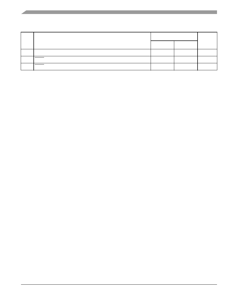
SJ11
TCK low to TDO high impedance
—
44
ns
SJ12
TRST assert time
100
—
ns
SJ13
TRST set-up time to TCK low
40
—
ns
1 On cases where SDMA TAP is put in the chain, the max TCK frequency is limited by max ratio of 1:8 of SDMA core frequency
to TCK limitation. This implies max frequency of 8.25 MHz (or 121.2 ns) for 66 MHz IPG clock.
2 V
M - mid point voltage
Table 56. SJC Timing Parameters (continued)
ID
Parameter
All Frequencies
Unit
Min
Max
相关PDF资料 |
PDF描述 |
|---|---|
| MCIMX31LCVMN4D | IC MPU I.MX31L AUTO 473MAPBGA |
| MCIMX31LCVMN4C | IC MPU MAP I.MX31L 473-MAPBGA |
| VE-J5B-IX-S | CONVERTER MOD DC/DC 95V 75W |
| VI-JNF-IX-S | CONVERTER MOD DC/DC 72V 75W |
| VI-JND-IX-S | CONVERTER MOD DC/DC 85V 75W |
相关代理商/技术参数 |
参数描述 |
|---|---|
| MCIMX31LCVMN4D | 功能描述:处理器 - 专门应用 2.0.1 AUTO LITE RoHS:否 制造商:Freescale Semiconductor 类型:Multimedia Applications 核心:ARM Cortex A9 处理器系列:i.MX6 数据总线宽度:32 bit 最大时钟频率:1 GHz 指令/数据缓存: 数据 RAM 大小:128 KB 数据 ROM 大小: 工作电源电压: 最大工作温度:+ 95 C 安装风格:SMD/SMT 封装 / 箱体:MAPBGA-432 |
| MCIMX31LCVMN4DR2 | 功能描述:处理器 - 专门应用 2.0.1 AUTO LITE RoHS:否 制造商:Freescale Semiconductor 类型:Multimedia Applications 核心:ARM Cortex A9 处理器系列:i.MX6 数据总线宽度:32 bit 最大时钟频率:1 GHz 指令/数据缓存: 数据 RAM 大小:128 KB 数据 ROM 大小: 工作电源电压: 最大工作温度:+ 95 C 安装风格:SMD/SMT 封装 / 箱体:MAPBGA-432 |
| MCIMX31LDVKN5D | 功能描述:处理器 - 专门应用 2.0.1 CONSUMER LITE RoHS:否 制造商:Freescale Semiconductor 类型:Multimedia Applications 核心:ARM Cortex A9 处理器系列:i.MX6 数据总线宽度:32 bit 最大时钟频率:1 GHz 指令/数据缓存: 数据 RAM 大小:128 KB 数据 ROM 大小: 工作电源电压: 最大工作温度:+ 95 C 安装风格:SMD/SMT 封装 / 箱体:MAPBGA-432 |
| MCIMX31LDVKN5DR2 | 功能描述:处理器 - 专门应用 2.0.1 CONSUMER LITE RoHS:否 制造商:Freescale Semiconductor 类型:Multimedia Applications 核心:ARM Cortex A9 处理器系列:i.MX6 数据总线宽度:32 bit 最大时钟频率:1 GHz 指令/数据缓存: 数据 RAM 大小:128 KB 数据 ROM 大小: 工作电源电压: 最大工作温度:+ 95 C 安装风格:SMD/SMT 封装 / 箱体:MAPBGA-432 |
| MCIMX31LDVMN5D | 功能描述:处理器 - 专门应用 2.0.1 CONSUMER LITE RoHS:否 制造商:Freescale Semiconductor 类型:Multimedia Applications 核心:ARM Cortex A9 处理器系列:i.MX6 数据总线宽度:32 bit 最大时钟频率:1 GHz 指令/数据缓存: 数据 RAM 大小:128 KB 数据 ROM 大小: 工作电源电压: 最大工作温度:+ 95 C 安装风格:SMD/SMT 封装 / 箱体:MAPBGA-432 |
发布紧急采购,3分钟左右您将得到回复。