- 您现在的位置:买卖IC网 > PDF目录1852 > MCP1253T-ADJI/MS (Microchip Technology)IC REG MULTI CONFIG ADJ 8MSOP PDF资料下载
参数资料
| 型号: | MCP1253T-ADJI/MS |
| 厂商: | Microchip Technology |
| 文件页数: | 9/18页 |
| 文件大小: | 0K |
| 描述: | IC REG MULTI CONFIG ADJ 8MSOP |
| 标准包装: | 2,500 |
| 类型: | 降压(降压),升压(升压),切换电容(充电泵) |
| 输出类型: | 可调式 |
| 输出数: | 1 |
| 输出电压: | 1.5 V ~ 5.5 V |
| 输入电压: | 2 V ~ 5.5 V |
| 频率 - 开关: | 1MHz |
| 电流 - 输出: | 120mA |
| 同步整流器: | 无 |
| 工作温度: | -40°C ~ 85°C |
| 安装类型: | 表面贴装 |
| 封装/外壳: | 8-TSSOP,8-MSOP(0.118",3.00mm 宽) |
| 包装: | 带卷 (TR) |
| 供应商设备封装: | 8-MSOP |
�� �
�
�MCP1252/3�
�4.0�
�DEVICE� OVERVIEW�
�4.1�
�Theory� of� Operation�
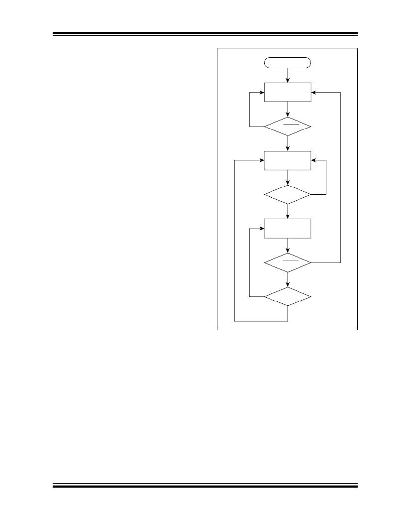
�START�
�The� MCP1252� and� MCP1253� family� of� devices� employ�
�a� switched� capacitor� charge� pump� to� buck� or� boost� an�
�input� supply� voltage� (V� IN� )� to� a� regulated� output� voltage.�
�Referring� to� the� Functional� Block� Diagram� and�
��tion� in� three� phases.� When� the� devices� are� not� in� shut-�
�PHASE� 1:�
�Charge� Transfer�
�From� V� IN� to� C� FLY�
�down� mode� and� a� steady-state� condition� has� been�
�reached,� the� three� phases� are� continuously� cycled�
�through.� The� first� phase� transfers� charge� from� the� input�
�to� the� flying� capacitor� (C� FLY� )� connected� to� pins� C+� and�
�C-.� This� phase� always� occurs� for� half� of� the� internal�
�oscillator� period.� During� this� phase,� switches� S� 1� and� S� 2�
�are� closed.�
�Once� the� first� phase� is� complete,� all� switches� are�
�opened� and� the� second� phase� (idle� phase)� is� entered.�
�No�
�1�
�t� 1� =� 2F� OSC�
�Yes�
�PHASE� 2:�
�Idle� State�
�The� device� compares� the� internal� or� external� feedback�
�voltage� with� an� internal� reference.� If� the� feedback� volt-�
�age� is� below� the� regulation� point,� the� device� transitions�
�to� the� third� phase.�
�The� third� phase� transfers� energy� from� the� flying� capac-�
�itor� to� the� output� capacitor� connected� to� V� OUT� and� the�
�load.� If� regulation� is� maintained,� the� device� returns� to�
�the� idle� phase.� If� the� charge� transfer� occurs� for� half� the�
�internal� oscillator� period,� more� charge� is� needed� in� the�
�flying� capacitor� and� the� device� transitions� back� to� the�
�first� phase.�
�The� regulation� control� is� hysteretic,� otherwise� referred�
�to� as� a� bang-bang� control.� The� output� is� regulated�
�around� a� fixed� reference� with� some� hysteresis.� As� a�
�V� FB� >� V� REF�
�No�
�PHASE� 3:�
�Charge� Transfer�
�From C� FLY� to C� OUT�
�1�
�t� 3� =� 2F� OSC�
�No�
�Yes�
�Yes�
�result,� typically� 50� mV� of� peak-to-peak� ripple� will� be�
�observed� at� the� output� independent� of� load� current.�
�The� frequency� of� the� output� ripple,� however,� will� be�
�influenced� heavily� by� the� load� current� and� output�
�capacitance.� The� maximum� frequency� that� will� be�
�observed� is� equal� to� the� internal� oscillator� frequency.�
�The� devices� automatically� transition� between� buck� or�
�boost� operation.� This� provides� a� low-cost,� compact� and�
�simple� solution� for� step-down/step-up� DC/DC� conver-�
�sion.� This� is� especially� true� for� battery-operated� appli-�
�cations� that� require� a� fixed� output� above� or� below� the�
�input.�
�?� 2002� Microchip� Technology� Inc.�
�No�
�Yes�
�FIGURE� 4-1:�
�V� FB� >� V� REF�
�Flow� Algorithm.�
�DS21752A-page� 9�
�相关PDF资料 |
PDF描述 |
|---|---|
| MCP131-270E/TO | IC SUPERVISOR 2.63V LOW TO-92 |
| MCP1318T-29HE/OT | IC SPRVSR SMPL RSET 2.9V SOT23-5 |
| MCP1416RT-E/OT | IC PWR MOSFET DVR 1.5A SOT23-5 |
| MCP1525-I/TO | IC VREF SERIES PREC 2.5V TO-92-3 |
| MCP1601T-I/MS | IC REG BUCK SYNC ADJ 0.5A 8MSOP |
相关代理商/技术参数 |
参数描述 |
|---|---|
| MCP1256 | 制造商:MICROCHIP 制造商全称:Microchip Technology 功能描述:Regulated 3.3V, Low-Ripple Charge Pump with Low- Operating Current SLEEP Mode or BYPASS Mode |
| MCP1256/7/8/9EV | 功能描述:电源管理IC开发工具 MCP1256/7/8/9 Eval Brd RoHS:否 制造商:Maxim Integrated 产品:Evaluation Kits 类型:Battery Management 工具用于评估:MAX17710GB 输入电压: 输出电压:1.8 V |
| MCP1256_13 | 制造商:MICROCHIP 制造商全称:Microchip Technology 功能描述:Regulated 3.3V, Low-Ripple Charge Pump with Low- Operating Current SLEEP Mode or BYPASS Mode |
| MCP1256-E/MF | 功能描述:电荷泵 Frac Charge Pump w/ PG and Sleep RoHS:否 制造商:Maxim Integrated 功能:Inverting, Step Up 输出电压:- 1.5 V to - 5.5 V, 3 V to 11 V 输出电流:100 mA 电源电流:1 mA 最大工作温度:+ 70 C 封装 / 箱体:SOIC-8 Narrow 封装:Tube |
| MCP1256-E/UN | 功能描述:电荷泵 Frac Charge Pump w/ PG and Sleep RoHS:否 制造商:Maxim Integrated 功能:Inverting, Step Up 输出电压:- 1.5 V to - 5.5 V, 3 V to 11 V 输出电流:100 mA 电源电流:1 mA 最大工作温度:+ 70 C 封装 / 箱体:SOIC-8 Narrow 封装:Tube |
发布紧急采购,3分钟左右您将得到回复。