- 您现在的位置:买卖IC网 > PDF目录296502 > MCP1700-3002ETO (Microchip Technology Inc.) Low Quiescent Current LDO PDF资料下载
参数资料
| 型号: | MCP1700-3002ETO |
| 厂商: | Microchip Technology Inc. |
| 元件分类: | 线性稳压 |
| 英文描述: | Low Quiescent Current LDO |
| 中文描述: | 低静态电流低压降稳压器 |
| 文件页数: | 16/22页 |
| 文件大小: | 522K |
| 代理商: | MCP1700-3002ETO |
2003 Microchip Technology Inc.
DS21826A-page 3
MCP1700
1.0
ELECTRICAL
CHARACTERISTICS
Absolute Maximum Ratings
VDD............................................................................................+6.5V
All inputs and outputs w.r.t. .............(VSS-0.3V) to (VIN+0.3V)
Peak Output Current .................................... Internally Limited
Storage temperature .....................................-65°C to +150°C
Maximum Junction Temperature................................... 150°C
Operating Junction Temperature...................-40°C to +125°C
ESD protection on all pins (HBM;MM)
............... ≥ 4kV; ≥ 400V
Notice: Stresses above those listed under “Maximum Rat-
ings” may cause permanent damage to the device. This is a
stress rating only and functional operation of the device at
those or any other conditions above those indicated in the
operational listings of this specification is not implied. Expo-
sure to maximum rating conditions for extended periods may
affect device reliability.
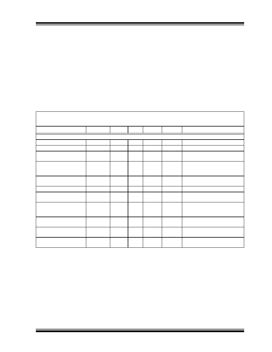
DC CHARACTERISTICS
Electrical Characteristics: Unless otherwise specified, all limits are established for VIN = VR + 1, ILOAD = 100 A, COUT = 1 F
(X5R), CIN = 1 F (X5R), TA = +25°C.
Boldface type applies for junction temperatures, TJ (Note 6) of -40°C to +125°C.
Parameters
Sym
Min
Typ
Max
Units
Conditions
Input / Output Characteristics
Input Operating Voltage
VIN
2.3
—
6.0
V
Input Quiescent Current
Iq
—1.6
4
A
IL = 0 mA, VIN = VR +1V
Maximum Output Current
IOUT_mA
250
200
—
mA
For VR ≥ 2.5V
For VR < 2.5V
Output Short Circuit Current
IOUT_SC
—408
—
mA
VIN = VR +1V, VOUT = GND,
Current (peak current) measured
10 ms after short is applied.
Output Voltage Regulation
VOUT
VR-3.0%
VR-2.0%
VR±0.4
%
VR+3.0%
VR+2.0%
V
VOUT Temperature Coefficient
TCVOUT
—50
—
ppm/°C
Line Regulation
VOUT/
(VOUTXVIN)
-1.0
±0.75
+1.0
%/V
(VR+1)V ≤ VIN ≤ 6V
Load Regulation
VOUT/VOUT
-1.5
±1.0
+1.5
%IL = 0.1 mA to 250 mA for VR ≥ 2.5V
IL = 0.1 mA to 200 mA for VR < 2.5V
Dropout Voltage
VR > 2.5V
VIN-VOUT
—178
350
mV
Dropout Voltage
VR < 2.5V
VIN-VOUT
—150
350
mV
Output Rise Time
TR
—
500
—
s
10% VR to 90% VR VIN = 0V to 6V,
RL = 50 resistive
Note 1:
The minimum VIN must meet two conditions: VIN ≥ 2.3V and VIN ≥ (VR + 3.0%) +VDROPOUT.
2:
VR is the nominal regulator output voltage. For example: VR = 1.2V, 1.5V, 1.8V, 2.5V, 2.8V, 3.0V, 3.3V, 4.0V, 5.0V. The
input voltage (VIN = VR + 1.0V); IOUT = 100 A.
3:
TCVOUT = (VOUT-HIGH - VOUT-LOW) *106 / (VR * Temperature), VOUT-HIGH = highest voltage measured over the
temperature range. VOUT-LOW = lowest voltage measured over the temperature range.
4:
Load regulation is measured at a constant junction temperature using low duty cycle pulse testing. Changes in output
voltage due to heating effects are determined using thermal regulation specification TCVOUT.
5:
Dropout voltage is defined as the input to output differential at which the output voltage drops 2% below its measured
value with a VR + 1V differential applied.
6:
The maximum allowable power dissipation is a function of ambient temperature, the maximum allowable junction
temperature and the thermal resistance from junction to air (i.e., TA, TJ, θJA). Exceeding the maximum allowable power
dissipation will cause the device operating junction temperature to exceed the maximum 150°C rating. Sustained
junction temperatures above 150°C can impact the device reliability.
7:
The junction temperature is approximated by soaking the device under test at an ambient temperature equal to the
desired Junction temperature. The test time is small enough such that the rise in the Junction temperature over the
ambient temperature is not significant.
相关PDF资料 |
PDF描述 |
|---|---|
| MCP1700-3302ETO | Low Quiescent Current LDO |
| MCP1700-5002ETO | Low Quiescent Current LDO |
| MCP1700T-3002ETT | Low Quiescent Current LDO |
| MCP1700T-3302EMB | Low Quiescent Current LDO |
| MCP1700T-3302ETO | Low Quiescent Current LDO |
相关代理商/技术参数 |
参数描述 |
|---|---|
| MCP1700-3102E/TO | 功能描述:低压差稳压器 - LDO 250mA CMOS LDO Isupp 1uA 2% Vout Acc RoHS:否 制造商:Texas Instruments 最大输入电压:36 V 输出电压:1.4 V to 20.5 V 回动电压(最大值):307 mV 输出电流:1 A 负载调节:0.3 % 输出端数量: 输出类型:Fixed 最大工作温度:+ 125 C 安装风格:SMD/SMT 封装 / 箱体:VQFN-20 |
| MCP1700-3302E/TO | 功能描述:低压差稳压器 - LDO 250mA LDO 2% RoHS:否 制造商:Texas Instruments 最大输入电压:36 V 输出电压:1.4 V to 20.5 V 回动电压(最大值):307 mV 输出电流:1 A 负载调节:0.3 % 输出端数量: 输出类型:Fixed 最大工作温度:+ 125 C 安装风格:SMD/SMT 封装 / 箱体:VQFN-20 |
| MCP1700-4002E/TO | 功能描述:低压差稳压器 - LDO 250mA CMOS LDO Isupp 1uA 2% Vout Acc RoHS:否 制造商:Texas Instruments 最大输入电压:36 V 输出电压:1.4 V to 20.5 V 回动电压(最大值):307 mV 输出电流:1 A 负载调节:0.3 % 输出端数量: 输出类型:Fixed 最大工作温度:+ 125 C 安装风格:SMD/SMT 封装 / 箱体:VQFN-20 |
| MCP1700-5002E/TO | 功能描述:低压差稳压器 - LDO 250mA Adj LDO 2% RoHS:否 制造商:Texas Instruments 最大输入电压:36 V 输出电压:1.4 V to 20.5 V 回动电压(最大值):307 mV 输出电流:1 A 负载调节:0.3 % 输出端数量: 输出类型:Fixed 最大工作温度:+ 125 C 安装风格:SMD/SMT 封装 / 箱体:VQFN-20 |
| MCP1700T-1202E/MB | 功能描述:低压差稳压器 - LDO 250mA Adj LDO 2% RoHS:否 制造商:Texas Instruments 最大输入电压:36 V 输出电压:1.4 V to 20.5 V 回动电压(最大值):307 mV 输出电流:1 A 负载调节:0.3 % 输出端数量: 输出类型:Fixed 最大工作温度:+ 125 C 安装风格:SMD/SMT 封装 / 箱体:VQFN-20 |
发布紧急采购,3分钟左右您将得到回复。