- 您现在的位置:买卖IC网 > PDF目录10454 > MCP2003A-E/P (Microchip Technology)IC TXRX LIN W/VREG 8PDIP PDF资料下载
参数资料
| 型号: | MCP2003A-E/P |
| 厂商: | Microchip Technology |
| 文件页数: | 2/34页 |
| 文件大小: | 0K |
| 描述: | IC TXRX LIN W/VREG 8PDIP |
| 产品培训模块: | Microchip MCP20xx LIN Transceiver Overview |
| 标准包装: | 60 |
| 系列: | * |
第1页当前第2页第3页第4页第5页第6页第7页第8页第9页第10页第11页第12页第13页第14页第15页第16页第17页第18页第19页第20页第21页第22页第23页第24页第25页第26页第27页第28页第29页第30页第31页第32页第33页第34页
MCP2003/4/3A/4A
DS22230D-page 10
2010-2011 Microchip Technology Inc.
Fault condition or by an external drive. While the
transmitter is disabled, the internal 30 k
Ω pull-up
resistor on the LBUS pin is also disconnected to reduce
current.
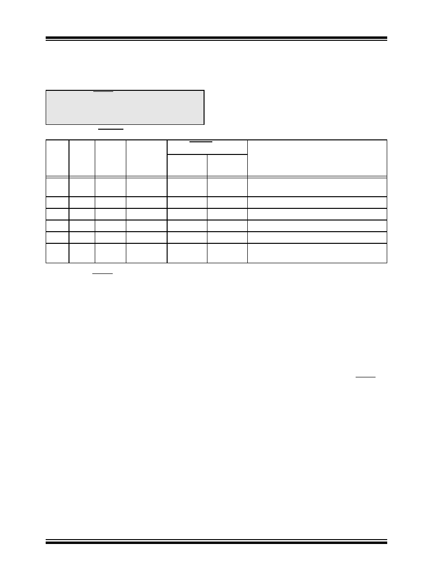
TABLE 1-3:
FAULT/TXE TRUTH TABLE
1.5.5
TRANSMIT DATA INPUT (TXD)
The Transmit Data Input pin has an internal pull-up.
The LIN pin is low (dominant) when TXD is low, and high
(recessive) when TXD is high.
For extra bus security, TXD is internally forced to ‘1’
whenever the transmitter is disabled regardless of
external TXD voltage.
1.5.5.1
TXD Dominant Timeout
If TXD is driven low for longer than approximately 25
mS, the LBUS pin is switched to recessive mode and
the part enters TOFF Mode. This is to prevent the LIN
node from permanently driving the LIN Bus dominant.
The transmitter is reenabled on TXD rising edge.
1.5.6
GROUND (VSS)
This is the Ground pin.
1.5.7
LIN BUS (LBUS)
The bidirectional LIN Bus pin (LBUS) is controlled by the
TXD input. LBUS has a current limited open collector
output. To reduce EMI, the edges during the signal
changes are slope controlled and include corner
rounding control for both falling and rising edges.
The internal LIN receiver observes the activities on the
LIN bus, and matches the output signal RXD to follow
the state of the LBUS pin.
1.5.7.1
Bus Dominant Timer
The Bus Dominant Timer is an internal timer that
deactivates the LBUS transmitter after approximately
25 milliseconds of dominant state on the LBUS pin. The
timer is reset on any recessive LBUS state.
The LIN bus transmitter will be reenabled after a
recessive state on the LBUS pin as long as CS is high.
Disabling can be caused by the LIN bus being
externally held dominant, or by TXD being driven low.
Additionally, on the MCP2004/2004A, the FAULT pin
will be driven low to indicate the Transmitter Off state.
1.5.8
BATTERY (VBB)
This is the Battery Positive Supply Voltage pin.
1.5.9
VOLTAGE REGULATOR ENABLE
OUTPUT (VREN)
This is the External Voltage Regulator Enable pin.
Open source output is pulled high to VBB in all modes,
except Power-Down.
1.5.10
EXPOSED THERMAL PAD (EP)
Do not electrically connect, or connect to Vss.
Note:
The FAULT/TXE pin is true (‘0’) whenever
the internal circuits have detected a short
or thermal excursion and have disabled
the LBUS output driver.
TXD
In
RXD
Out
LINBUS
I/O
Thermal
Override
FAULT/TXE
Definition
External
Input
Driven
Output
LH
VBB
OFF
H
L
FAULT, TXD driven low, LINBUS shorted to VBB
HH
VBB
OFF
H
OK
L
GND
OFF
H
OK
H
L
GND
OFF
H
OK, data is being received from the LINBUS
xx
VBB
ON
H
L
FAULT, Transceiver in thermal shutdown
xx
VBB
x
L
x
NO FAULT, the CPU is commanding the
transceiver to turn off the transmitter driver
Legend: x = don’t care
Note 1:
The FAULT/TXE is valid after approximately 25 s after TXD falling edge. This is to eliminate false fault
reporting during bus propagation delays.
相关PDF资料 |
PDF描述 |
|---|---|
| MCP2004AT-E/SN | IC TXRX LIN W/VREG 8SOIC |
| VE-26N-IU | CONVERTER MOD DC/DC 18.5V 200W |
| MCP2003AT-E/SN | IC TXRX LIN W/VREG 8SOIC |
| VE-26K-IU | CONVERTER MOD DC/DC 40V 200W |
| VE-26H-IU | CONVERTER MOD DC/DC 52V 200W |
相关代理商/技术参数 |
参数描述 |
|---|---|
| MCP2003AT-E/MD | 功能描述:LIN 收发器 Stand alone LIN Transceiver RoHS:否 制造商:NXP Semiconductors 工作电源电压: 电源电流: 最大工作温度: 封装 / 箱体:SO-8 |
| MCP2003AT-E/SN | 功能描述:LIN 收发器 Stand alone LIN Transceiver RoHS:否 制造商:NXP Semiconductors 工作电源电压: 电源电流: 最大工作温度: 封装 / 箱体:SO-8 |
| MCP2003-E/MD | 功能描述:LIN 收发器 Stand Alone LIN Transceiver RoHS:否 制造商:NXP Semiconductors 工作电源电压: 电源电流: 最大工作温度: 封装 / 箱体:SO-8 |
| MCP2003-E/P | 功能描述:LIN 收发器 Stand Alone LIN Transceiver RoHS:否 制造商:NXP Semiconductors 工作电源电压: 电源电流: 最大工作温度: 封装 / 箱体:SO-8 |
| MCP2003-E/SN | 功能描述:LIN 收发器 Stand Alone LIN Transceiver RoHS:否 制造商:NXP Semiconductors 工作电源电压: 电源电流: 最大工作温度: 封装 / 箱体:SO-8 |
发布紧急采购,3分钟左右您将得到回复。