- 您现在的位置:买卖IC网 > PDF目录10598 > MCP201-I/P (Microchip Technology)IC LIN TXRX ON-BOARD VREG 8DIP PDF资料下载
参数资料
| 型号: | MCP201-I/P |
| 厂商: | Microchip Technology |
| 文件页数: | 38/40页 |
| 文件大小: | 0K |
| 描述: | IC LIN TXRX ON-BOARD VREG 8DIP |
| 产品培训模块: | Microchip MCP20xx LIN Transceiver Overview |
| 标准包装: | 60 |
| 类型: | 线路收发器 |
| 驱动器/接收器数: | 1/1 |
| 规程: | LIN |
| 电源电压: | 6 V ~ 18 V |
| 安装类型: | 通孔 |
| 封装/外壳: | 8-DIP(0.300",7.62mm) |
| 供应商设备封装: | 8-PDIP |
| 包装: | 管件 |
| 产品目录页面: | 685 (CN2011-ZH PDF) |
第1页第2页第3页第4页第5页第6页第7页第8页第9页第10页第11页第12页第13页第14页第15页第16页第17页第18页第19页第20页第21页第22页第23页第24页第25页第26页第27页第28页第29页第30页第31页第32页第33页第34页第35页第36页第37页当前第38页第39页第40页
2007 Microchip Technology Inc.
DS21730F-page 7
MCP201
1.5
Pin Descriptions
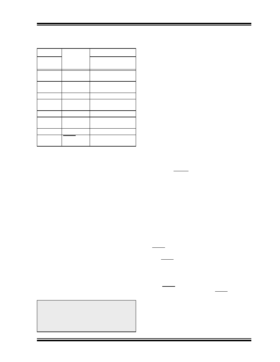
TABLE 1-3:
MCP201 PINOUT OVERVIEW
1.5.1
RECEIVE DATA OUTPUT (RXD)
The Receive Data Output pin is a standard CMOS
output and follows the state of the LIN pin.
The LIN receiver monitors the state of the LIN pin and
generates the output signal RXD.
1.5.2
CS/WAKE
Chip Select Input pin. This pin controls whether the part
goes into READY1 or READY mode at power-up. The
internal pull-down resistor will keep the CS/WAKE pin
low. This is done to ensure that no disruptive data will
be present on the bus while the microcontroller is
executing a Power-on Reset and I/O initialization
sequence. The pin must see a low-to-high transition to
activate the transmitter.
After CS/WAKE transitions to ‘1’, the transmitter is
enabled. If CS/WAKE = ‘0’, the device is in Ready1
mode on power-up or in Low-Power mode. In Low-
Power mode, the voltage regulator is shut down, the
transmitter driver is disabled and the receiver logic is
enabled.
An external switch (see Figure 1-2) can then wake up
both the transceiver and the microcontroller. An
external-blocking diode and current-limiting resistor are
necessary to protect the microcontroller I/O pin.
1.5.3
POWER OUTPUT (VREG)
Positive Supply Voltage Regulator Output pin.
1.5.4
TRANSMIT DATA INPUT (TXD)
The Transmit Data Input pin has an internal pull-up to
VREG. The LIN pin is low (dominant) when TXD is low,
and high (recessive) when TXD is high.
In case the thermal protection detects an over-temper-
ature condition while the signal TXD is low, the
transmitter is shutdown. The recovery from the thermal
shutdown is equal to adequate cooling time.
1.5.5
GROUND (VSS)
Ground pin.
1.5.6
LIN
The bidirectional LIN bus Interface pin is the driver unit
for the LIN pin and is controlled by the signal TXD. LIN
has an open collector output with a current limitation.
To reduce EMI, the edges during the signal changes
are slope-controlled.
1.5.7
BATTERY (VBAT)
Battery Positive Supply Voltage pin. This pin is also the
input for the internal voltage regulator.
1.5.8
FAULT/SLPS
FAULT Detect Output, Slope Select Input.
This pin is usually in Output mode. Its state is defined
as shown in Table 1-5.
The state of this pin is internally sampled during power-
on of VBAT. Once VBAT has reached a stable level,
(approximately 6 VDC) and VREG is stable at 4.75 to
5.25 VDC, the state of this pin selects which slew rate
profile to apply to the LIN output. It is only during this
time that the pin is used as an input (the output driver
is off during this time). The slope will stay selected until
the next VBAT power-off/power-on sequence, regard-
less of any power-down, wake-up or SLEEP events.
Only a VBAT rising state will cause a sampling of the
FAULT/SLPS pin. The Slope selection will be made
irrespective of the state of any other pin.
The FAULT/SLPS pin is connected to either VREG or
VSS through a resistor (approximately 100 k
Ω) to make
the slope selection. This large resistance allows the
FAULT indication function to overdrive the resistor in
normal operation mode.
If the FAULT/SLPS is high (‘1’), the normal slope shap-
ing is selected (dv/dt = 2 V/s). If FAULT/SLPS is low
(‘0’) during this time, the alternate slope-shaping is
selected (dv/dt = 4 V/s). This mode can be used if a
user desires to run at a faster slope. This mode is not
LIN compliant.
Devices
Bond Pad
Name
Function
8-Pin PDIP/
SOIC/DFN
Normal Operation
1
RXD
Receive Data Output
(CMOS output)
2
CS/WAKE
Chip Select (TTL-HV
input)
3VREG
Power Output
4
TXD
Transmit Data Input
(TTL)
5VSS
Ground
6
LIN
LIN bus (bidirectional-
HV)
7VBAT
Battery
8FAULT/SLPS
Fault Detect Output,
Slope Select Input
Legend: TTL = TTL input buffer,
HV = High Voltage (VBAT)
Note:
On POR, the MCP201 enters Ready or
Ready1 mode (see Figure 1-1). In order to
enter Operational mode, the MCP201 has
to see one rising edge on CS/WAKE
600 s after the voltage regulator reaches
5V.
相关PDF资料 |
PDF描述 |
|---|---|
| VI-JTT-MY-F4 | CONVERTER MOD DC/DC 6.5V 50W |
| VI-BW4-IV-F3 | CONVERTER MOD DC/DC 48V 150W |
| 85106JC1832P50 | CONN PLUG STRAIGHT 32POS W/PIN |
| 85106JC168P50 | CONN PLUG STRAIGHT 8POS W/PIN |
| AD9928BBCZRL | IC CCD SIGNAL PROCESSR 128CSPBGA |
相关代理商/技术参数 |
参数描述 |
|---|---|
| MCP201ISN | 制造商:Microchip Technology Inc 功能描述: |
| MCP201-ISN | 制造商:MICROCHIP 制造商全称:Microchip Technology 功能描述:LIN Transceiver with Voltage Regulator |
| MCP201T-E/SN | 功能描述:LIN 收发器 W/ On Board Vreg RoHS:否 制造商:NXP Semiconductors 工作电源电压: 电源电流: 最大工作温度: 封装 / 箱体:SO-8 |
| MCP201T-EMF | 制造商:MICROCHIP 制造商全称:Microchip Technology 功能描述:LIN Transceiver with Voltage Regulator |
| MCP201T-ESN | 制造商:MICROCHIP 制造商全称:Microchip Technology 功能描述:LIN Transceiver with Voltage Regulator |
发布紧急采购,3分钟左右您将得到回复。