- 您现在的位置:买卖IC网 > PDF目录10410 > MCP2022AT-500E/ST (Microchip Technology)IC TXRX LIN 5.0V LDO 14-TSSOP PDF资料下载
参数资料
| 型号: | MCP2022AT-500E/ST |
| 厂商: | Microchip Technology |
| 文件页数: | 23/48页 |
| 文件大小: | 0K |
| 描述: | IC TXRX LIN 5.0V LDO 14-TSSOP |
| 产品培训模块: | Microchip MCP20xx LIN Transceiver Overview |
| 标准包装: | 2,500 |
| 系列: | * |
第1页第2页第3页第4页第5页第6页第7页第8页第9页第10页第11页第12页第13页第14页第15页第16页第17页第18页第19页第20页第21页第22页当前第23页第24页第25页第26页第27页第28页第29页第30页第31页第32页第33页第34页第35页第36页第37页第38页第39页第40页第41页第42页第43页第44页第45页第46页第47页第48页
2012 Microchip Technology Inc.
DS22298A-page 3
MCP2021A/2A
1.0
FUNCTION DESCRIPTION
The MCP2021A/2A provides a physical interface
between a microcontroller and a LIN half-duplex bus. It
is intended for automotive and industrial applications
with serial bus baud rates up to 20 Kbaud. This device
will translate the CMOS/TTL logic levels to LIN logic
levels, and vice versa. The device offers optimum EMI
and ESD performance; it can withstand high voltage on
the LIN bus. The device supports two low-power
modes to meet automotive industry power consump-
tion requirements. The MCP2021A/2A also provides a
+5V or 3.3V 70 mA regulated power output.
1.1
Modes of Operation
The MCP2021A/2A works in five modes: POWER-ON-
RESET mode, POWER-DOWN mode, READY mode,
OPERATION mode, and TRANSMITTER OFF mode.
For an overview of all operational modes, please refer
to Table 1-1. For the operational mode transition,
please refer to Figure 1-1.
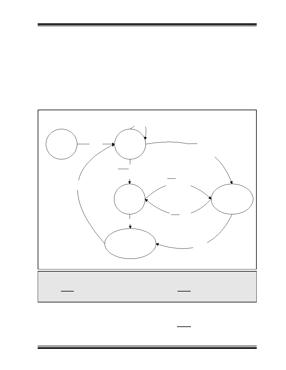
FIGURE 1-1:
STATE DIAGRAM
1.1.1
POWER-ON-RESET MODE
Upon application of VBB, or whenever the voltage on
VBB is below the threshold of regulator turn off voltage
VOFF (typically 4.50V), the device enters POWER-ON-
RESET mode (POR). During this mode, the device
maintains the digital section in a reset mode and waits
until the voltage on VBB pin rises above the threshold of
regulator turn on voltage VON (typically 5.75V) to enter
to the READY mode. In POWER-ON-RESET mode,
the LIN physical layer and voltage regulator are dis-
abled, and RESET output (MCP2022A only) is forced
to LOW.
POR
(2)
VREG OFF
RX OFF
TX OFF
READY
VREG ON
RX ON
TX OFF
TX OFF
VREG ON
RX ON
TX OFF
POWER-DOWN
VREG OFF
RX OFF
TX OFF
OPERATION
VREG ON
RX ON
TX ON
VBB>VON
CS/LWAKE=1&
FAULT/TXE=0&
VREG_OK=1
(1)
CS/LWAKE=0
CS/LWAKE=1 &
FAULT/TXE=1
(3) &
TXD=1&
VREG_OK=1
(1)
CS/LWAKE=1&
FAULT/TXE=1
(3)&
TXD=1
CS/LWAKE=1&
FAULT/TXE=0
CS/LWAKE=0
CS/LWAKE=1 OR
Voltage Rising Edge on LBUS
CS/LWAKE=0
Note 1: VREG_OK : Regulator Output Voltage > 0.8VREG_NOM.
2: If the voltage on pin VBB falls below VOFF, the device will enter POWER ON RESET mode from all other
modes, which is not shown in the figure.
3: FAULT/TXE = 1 represents input high and no fault conditions. FAULT/TXE = 0 represents input low or a
fault condition, Refer to Table 1-3.
相关PDF资料 |
PDF描述 |
|---|---|
| MCP2022AT-330E/ST | IC TXRX LIN 3.3V LDO 14-TSSOP |
| VE-BN3-MW | CONVERTER MOD DC/DC 24V 100W |
| 17292-3SG-3ES | CONN RCPT 3POS PNL MNT SKT |
| VE-BN2-MX-F4 | CONVERTER MOD DC/DC 15V 75W |
| VE-BN1-MX-F3 | CONVERTER MOD DC/DC 12V 75W |
相关代理商/技术参数 |
参数描述 |
|---|---|
| MCP2022P | 制造商:MICROCHIP 制造商全称:Microchip Technology 功能描述:LIN Transceiver with Voltage Regulator |
| MCP2022P-330E/SL | 功能描述:LIN 收发器 LIN Transceiver with Vreg and LIN RoHS:否 制造商:NXP Semiconductors 工作电源电压: 电源电流: 最大工作温度: 封装 / 箱体:SO-8 |
| MCP2022P-330E/ST | 功能描述:LIN 收发器 LIN Transceiver with Vreg and LIN RoHS:否 制造商:NXP Semiconductors 工作电源电压: 电源电流: 最大工作温度: 封装 / 箱体:SO-8 |
| MCP2022P-500E/SL | 功能描述:LIN 收发器 LIN Transceiver with Vreg and LIN RoHS:否 制造商:NXP Semiconductors 工作电源电压: 电源电流: 最大工作温度: 封装 / 箱体:SO-8 |
| MCP2022P-500E/ST | 功能描述:LIN 收发器 LIN Transceiver with Vreg and LIN RoHS:否 制造商:NXP Semiconductors 工作电源电压: 电源电流: 最大工作温度: 封装 / 箱体:SO-8 |
发布紧急采购,3分钟左右您将得到回复。