- 您现在的位置:买卖IC网 > PDF目录17040 > MCP355XDV-MS1 (Microchip Technology)BOARD DEV SENSOR APP MCP355X PDF资料下载
参数资料
| 型号: | MCP355XDV-MS1 |
| 厂商: | Microchip Technology |
| 文件页数: | 11/36页 |
| 文件大小: | 0K |
| 描述: | BOARD DEV SENSOR APP MCP355X |
| 产品培训模块: | MCP3901 Analog Front End |
| 标准包装: | 1 |
| ADC 的数量: | 1 |
| 位数: | 22 |
| 数据接口: | 串行 |
| 输入范围: | ±0.3 V |
| 工作温度: | -40°C ~ 125°C |
| 已用 IC / 零件: | MCP355x |
| 已供物品: | 板,CD,样品 |
| 产品目录页面: | 672 (CN2011-ZH PDF) |
| 相关产品: | MCP3550T-60E/SN-ND - IC ADC 22BIT 2.7V 1CH 8SOIC MCP3550T-60E/MS-ND - IC ADC 22BIT 2.7V 1CH 8MSOP MCP3550T-50E/SN-ND - IC ADC 22BIT 2.7V 1CH 8SOIC MCP3550T-50E/MS-ND - IC ADC 22BIT 2.7V 1CH 8MSOP MCP3550-60E/SN-ND - IC ADC 22BIT 2.7V 1CH 8SOIC MCP3550-60E/MS-ND - IC ADC 22BIT 2.7V 1CH 8MSOP MCP3550-50E/SN-ND - IC ADC 22BIT 2.7V 1CH 8SOIC MCP3550-50E/MS-ND - IC ADC 22BIT 2.7V 1CH 8MSOP MCP3553T-E/SN-ND - IC ADC 22BIT 2.7V 1CH SPI 8SOIC MCP3553T-E/MS-ND - IC ADC 22BIT 2.7V 1CH SPI 8MSOP 更多... |
第1页第2页第3页第4页第5页第6页第7页第8页第9页第10页当前第11页第12页第13页第14页第15页第16页第17页第18页第19页第20页第21页第22页第23页第24页第25页第26页第27页第28页第29页第30页第31页第32页第33页第34页第35页第36页
2009 Microchip Technology Inc.
DS21950E-page 19
MCP3550/1/3
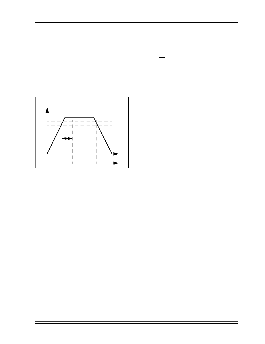
Once a power-up event has occurred, the device must
require additional time before a conversion can take
place. During this time, all internal analog circuitry must
settle before the first conversion can occur. An internal
timer counts 32 internal clock periods before the
internal oscillator can provide clock to the conversion
process. This allows all internal analog circuitry to
settle to their proper operating point. This timing is
typically less than 300 s, which is negligible compared
to one conversion time (e.g. 72.7 ms for the
MCP3551). Figure 4-6 illustrates the conditions for a
power-up and power-down event under typical start-up
conditions.
FIGURE 4-6:
Power-On Reset Operation.
4.7
Shutdown Mode
When not internally converting, the two modes of
operation for the MCP3550/1/3 devices are the
Shutdown and Sleep modes. During Shutdown mode,
all internal analog circuitry, including the POR, is turned
off and the device consumes less than 1 A. When
exiting Shutdown mode, the device must require
additional time before a conversion can take place.
During this time, all internal analog circuitry must settle
before the first conversion can occur. An internal timer
counts 32 internal clock periods before the internal
oscillator can provide clock to the conversion process.
This allows all internal analog circuitry to settle to their
proper operating point. This timing is typically less than
300 s, which is negligible compared to one conversion
time (72.7 ms for MCP3551).
4.8
Sleep Mode
During Sleep mode, the device is not converting and is
awaiting data retrieval; the internal analog circuitry is
still running and the device typically consumes 10 A.
In order to restart a conversion while in Sleep mode,
toggling CS to a logic-high (placing the part in Shut-
down mode) and then back to a logic-low will restart the
conversion. Sleep can only be entered in Single
Conversion mode. Once a conversion is complete in
Single Conversion mode, the device automatically
enters Sleep mode.
VDD
2.2V
2.0V
0V
Reset
Normal
Operation
Reset
Start-up
Time
300 s
相关PDF资料 |
PDF描述 |
|---|---|
| UPB2D681MRD | CAP ALUM 680UF 200V 20% RADIAL |
| MLG1005S68NJ | INDUCTOR MULTILAYER 68NH 0402 |
| GCC06DRYI-S93 | CONN EDGECARD 12POS DIP .100 SLD |
| EVAL-AD7658CBZ | BOARD EVAL FOR AD7658 |
| MCP3901EV-MCU16 | BOARD EVAL FOR 2CH ADC MCP3901 |
相关代理商/技术参数 |
参数描述 |
|---|---|
| MCP3901 | 制造商:MICROCHIP 制造商全称:Microchip Technology 功能描述:Two Channel Analog Front End |
| MCP3901_10 | 制造商:MICROCHIP 制造商全称:Microchip Technology 功能描述:Two-Channel Analog Front End |
| MCP3901_11 | 制造商:MICROCHIP 制造商全称:Microchip Technology 功能描述:Two-Channel Analog Front End Portable Instrumentation |
| MCP3901_12 | 制造商:MICROCHIP 制造商全称:Microchip Technology 功能描述:Energy Meter Reference Design |
| MCP3901A0-E/ML | 功能描述:模数转换器 - ADC Dual Ch Energy Meter Frnt End SPI I-face RoHS:否 制造商:Texas Instruments 通道数量:2 结构:Sigma-Delta 转换速率:125 SPs to 8 KSPs 分辨率:24 bit 输入类型:Differential 信噪比:107 dB 接口类型:SPI 工作电源电压:1.7 V to 3.6 V, 2.7 V to 5.25 V 最大工作温度:+ 85 C 安装风格:SMD/SMT 封装 / 箱体:VQFN-32 |
发布紧急采购,3分钟左右您将得到回复。