- 您现在的位置:买卖IC网 > PDF目录2013 > MCP3903T-E/SS (Microchip Technology)IC AFE 24BIT 64KSPS 6CH 28SSOP PDF资料下载
参数资料
| 型号: | MCP3903T-E/SS |
| 厂商: | Microchip Technology |
| 文件页数: | 10/15页 |
| 文件大小: | 0K |
| 描述: | IC AFE 24BIT 64KSPS 6CH 28SSOP |
| 产品培训模块: | MCP3903 6-Channel Energy Measurement Analog Front End |
| 标准包装: | 2,100 |
| 位数: | 24 |
| 通道数: | 6 |
| 电压 - 电源,模拟: | 4.5 V ~ 5.5 V |
| 电压 - 电源,数字: | 2.7 V ~ 3.6 V |
| 封装/外壳: | 28-SSOP(0.209",5.30mm 宽) |
| 供应商设备封装: | 28-SSOP |
| 包装: | 带卷 (TR) |
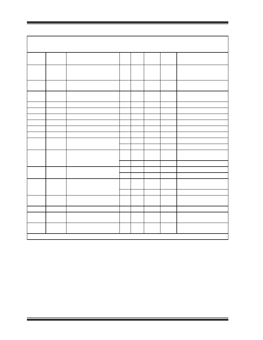
MCP3903
DS25048B-page 4
2011 Microchip Technology Inc.
A011
CHn+-
Analog Input Absolute
Voltage
-1
+1
V
All analog input channels,
measured to AGND
A012
AIN
Analog Input Leakage
Current
1nA
A013
(CHn+-
CHn-)
Differential Input Voltage
Range
500 /
GAIN
mVP
A014
VOS
Offset Error
-3
3
mV
A015
Offset Error Drift
1
μV/C
From -40°C to 125°C
A016
GE
Gain Error
-3
3
%
All Gains
A017
Gain Error Drift
—
2
—
ppm/°C From -40°C to 125°C
A018
INL
Integral Non-Linearity
15
ppm
GAIN = 1, DITHER = ON
A019
ZIN
Input Impedance
350
—
k
Ω
Proportional to 1/AMCLK
A020
SINAD
Signal-to-Noise and
Distortion Ratio
89
91
—
dB
T = 25°C
80
81.5
dB
A021
THD
Total Harmonic Distortion
-100
-97
dB
OSR = 256, DITHER = ON;
-90
-87
dB
A022
SNR
Signal To Noise Ratio
90
91.5
dB
T = 25°C
80
81.5
dB
A023
SFDR
Spurious Free Dynamic
Range
102
dB
OSR = 256, DITHER = ON;
91
dB
A024
CTALK
Crosstalk (50 / 60 Hz)
—
-115
—
dB
OSR = 256, DITHER = ON;
A025
AC PSRR AC Power Supply Rejection
—
-68
—
dB
AVDD = 5V + 1Vpp @ 50 Hz
A026
DC PSRR DC Power Supply Rejection
—
-68
—
dB
AVDD = 4.5 to 5.5V, DVDD =
3.3V
A027
CMRR
DC Common Mode Rejection
Ratio
—-75
—
dB
VCM varies from -1V to +1V;
Oscillator Input
TABLE 1-1:
ANALOG SPECIFICATIONS TARGET TABLE
(CONTINUED)
Electrical Specifications:
Unless otherwise indicated, all parameters apply at AVDD = 4.5 to 5.5V, DVDD = 2.7 to
3.6V, Internal VREF, MCLK = 4 MHz;PRESCALE = 1; OSR = 64; fS = 1 MHz; fD = 15.625 ksps; TA = -40°C to +125°C,
GAIN = 1, VIN = 1VPP = 353mVRMS @ 50/60 Hz.
Param.
Num.
Symbol
Characteristic
Min.
Typ.
Max.
Units
Test Conditions
Note 1:
This specification implies that the ADC output is valid over this entire differential range, i.e. there is no distortion or
instability across this input range. Dynamic Performance is specified at -0.5 dB below the maximum signal range,
VIN = -0.5 dBFS @ 50/60 Hz = 333 mVRMS, VREF = 2.4V.
2:
See terminology section for definition.
3:
This parameter is established by characterization and not 100% tested.
4:
For these operating currents, the following configuration bit settings apply: Config Register Settings:
SHUTDOWN<5:0> = 000000, RESET<5:0> = 000000; VREFEXT = 0, CLKEXT = 0.
5:
For these operating currents, the following configuration bit settings apply: Config Register Settings:
SHUTDOWN<5:0> = 111111, VREFEXT = 1, CLKEXT = 1.
6:
Applies to all gains. Offset error is dependant on PGA gain setting.
7:
Outside of this range, ADC accuracy is not specified. An extended input range of +/- 6V can be applied continuously to
the part with no risk for damage.
8:
For proper operation and to keep ADC accuracy, AMCLK should always be in the range of 1 to 5 MHz with BOOST bits
off. With BOOST bits on, AMCLK should be in the range of 1 to 8.192 MHz. AMCLK = MCLK/PRESCALE. When using a
crystal, CLKEXT bit should be equal to ‘0’.
相关PDF资料 |
PDF描述 |
|---|---|
| MCP3911A0T-E/ML | IC AFE 24BIT 125KSPS 2CH 20-QFN |
| MCP4725A3T-E/CH | IC DAC 12BIT EE W/I2C SOT23-6 |
| MCP4726A3T-E/CH | IC DAC 12BIT NV EEP I2C SOT-23-6 |
| MCP4728T-E/UN | IC DAC 12BIT W/I2C 10-MSOP |
| MCP4822T-E/MS | IC DAC 12BIT DUAL W/SPI 8MSOP |
相关代理商/技术参数 |
参数描述 |
|---|---|
| MCP3903T-I/SS | 功能描述:模数转换器 - ADC 6CH Energy Meter Front End SPI I-face RoHS:否 制造商:Texas Instruments 通道数量:2 结构:Sigma-Delta 转换速率:125 SPs to 8 KSPs 分辨率:24 bit 输入类型:Differential 信噪比:107 dB 接口类型:SPI 工作电源电压:1.7 V to 3.6 V, 2.7 V to 5.25 V 最大工作温度:+ 85 C 安装风格:SMD/SMT 封装 / 箱体:VQFN-32 |
| MCP3905 | 制造商:MICROCHIP 制造商全称:Microchip Technology 功能描述:Energy-Metering ICs with Active (Real) Power Pulse Output |
| MCP3905_07 | 制造商:MICROCHIP 制造商全称:Microchip Technology 功能描述:Energy-Metering ICs with Active (Real) Power Pulse Output |
| MCP3905_09 | 制造商:MICROCHIP 制造商全称:Microchip Technology 功能描述:Energy-Metering ICs with Active (Real) Power Pulse Output |
| MCP3905A | 制造商:MICROCHIP 制造商全称:Microchip Technology 功能描述:Energy Metering ICs with Active Real Power Pulse Output |
发布紧急采购,3分钟左右您将得到回复。