参数资料
| 型号: | MCP4561T-502E/MS |
| 厂商: | Microchip Technology |
| 文件页数: | 42/92页 |
| 文件大小: | 0K |
| 描述: | IC POT DGTL 5K SGL 8-MSOP |
| 标准包装: | 2,500 |
| 接片: | 257 |
| 电阻(欧姆): | 5k |
| 电路数: | 1 |
| 温度系数: | 标准值 150 ppm/°C |
| 存储器类型: | 非易失 |
| 接口: | I²C(设备位址) |
| 电源电压: | 2.7 V ~ 5.5 V |
| 工作温度: | -40°C ~ 125°C |
| 安装类型: | 表面贴装 |
| 封装/外壳: | 8-TSSOP,8-MSOP(0.118",3.00mm 宽) |
| 供应商设备封装: | 8-MSOP |
| 包装: | 带卷 (TR) |
第1页第2页第3页第4页第5页第6页第7页第8页第9页第10页第11页第12页第13页第14页第15页第16页第17页第18页第19页第20页第21页第22页第23页第24页第25页第26页第27页第28页第29页第30页第31页第32页第33页第34页第35页第36页第37页第38页第39页第40页第41页当前第42页第43页第44页第45页第46页第47页第48页第49页第50页第51页第52页第53页第54页第55页第56页第57页第58页第59页第60页第61页第62页第63页第64页第65页第66页第67页第68页第69页第70页第71页第72页第73页第74页第75页第76页第77页第78页第79页第80页第81页第82页第83页第84页第85页第86页第87页第88页第89页第90页第91页第92页
2008 Microchip Technology Inc.
DS22107A-page 47
MCP454X/456X/464X/466X
6.0
SERIAL INTERFACE (I2C)
The MCP45XX/46XX devices support the I2C serial
protocol. The MCP45XX/46XX I2C’s module operates
in Slave mode (does not generate the serial clock).
I2C interface signals are high-voltage tolerant.
The MCP45XX/46XX devices use the two-wire I2C
serial interface. This interface can operate in standard,
fast or High-Speed mode. A device that sends data
onto the bus is defined as transmitter, and a device
receiving data as receiver. The bus has to be controlled
by a master device which generates the serial clock
(SCL), controls the bus access and generates the
START and STOP conditions. The MCP45XX/46XX
device works as slave. Both master and slave can
operate as transmitter or receiver, but the master
device determines which mode is activated. Communi-
cation is initiated by the master (microcontroller) which
sends the START bit, followed by the slave address
byte. The first byte transmitted is always the slave
address byte, which contains the device code, the
address bits, and the R/W bit.
Refer to the Phillips I2C document for more details of
the I2C specifications.
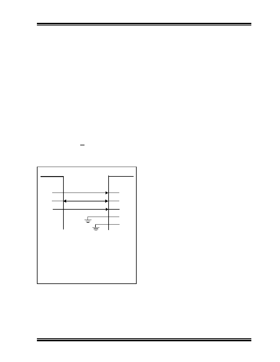
FIGURE 6-1:
Typical I2C Interface Block
Diagram.
6.1
Signal Descriptions
The I2C interface uses up to five pins (signals). These
are:
SDA (Serial Data)
SCL (Serial Clock)
A0 (Address 0 bit)
A1 (Address 1 bit)
A2 (Address 2 bit)
6.1.1
SERIAL DATA (SDA)
The Serial Data (SDA) signal is the data signal of the
device. The value on this pin is latched on the rising
edge of the SCL signal when the signal is an input.
With the exception of the START and STOP conditions,
the high or low state of the SDA pin can only change
when the clock signal on the SCL pin is low. During the
high period of the clock the SDA pin’s value (high or
low) must be stable. Changes in the SDA pin’s value
while the SCL pin is HIGH will be interpreted as a
START or a STOP condition.
6.1.2
SERIAL CLOCK (SCL)
The Serial Clock (SCL) signal is the clock signal of the
device. The rising edge of the SCL signal latches the
value on the SDA pin. The MCP45XX/46XX supports
three I2C interface clock modes:
Standard Mode: clock rates up to 100 kHz
Fast Mode: clock rates up to 400 kHz
High-Speed Mode (HS mode): clock rates up to
3.4 MHz
The MCP4XXX will not strech the clock signal (SCL)
since memory read acceses occur fast enough.
Depending on the clock rate mode, the interface will
display different characteristics.
6.1.3
THE ADDRESS BITS (A2:A1:A0)
There are up to three hardware pins used to specify the
device address. The number of adress pins is
determined by the part number.
Address 0 is multiplexed with the High Voltage
Command (HVC) function. So the state of A0 is latched
on the MCP4XXX’s POR/BOR event.
The state of the A2 and A1 pins should be static, that is
they should be tied high or tied low.
6.1.3.1
The High Voltage Command (HVC)
Signal
The High Voltage Command (HVC) signal is multi-
plexed with Address 0 (A0) and is used to indicate that
the command, or sequence of commands, are in the
High Voltage mode. High Voltage commands allow the
device’s WiperLock Technology and write protect
features to be enabled and disabled.
The HVC pin has an internal resistor connection to the
MCP45XX/46XXs internal VDD signal.
SCL
MCP4XXX
SDA
HVC/A0 (2)
I/O (1)
Host
Controller
Typical I2C Interface Connections
Note 1: If High voltage commands are desired,
some type of external circuitry needs to
be implemented.
2: These pins have internal pull-ups. If
faster rise times are required, then
external pull-ups should be added.
3: This pin could be tied high, low, or
connected to an I/O pin of the Host
Controller.
A1 (2, 3)
A2 (2, 3)
相关PDF资料 |
PDF描述 |
|---|---|
| MCP4562T-503E/MS | IC POT DGTL 50K SGL 8-MSOP |
| MCP4562T-104E/MS | IC POT DGTL 100K SGL 8-MSOP |
| VI-2NH-MY-F2 | CONVERTER MOD DC/DC 52V 50W |
| MCP4562T-502E/MS | IC POT DGTL 5K SGL 8-MSOP |
| MS3456W20-7SX | CONN PLUG 8POS STRAIGHT W/SCKT |
相关代理商/技术参数 |
参数描述 |
|---|---|
| MCP4561T-503E/MF | 功能描述:数字电位计 IC Sngl 8B NV I2C POT RoHS:否 制造商:Maxim Integrated 电阻:200 Ohms 温度系数:35 PPM / C 容差:25 % POT 数量:Dual 每 POT 分接头:256 弧刷存储器:Volatile 缓冲刷: 数字接口:Serial (3-Wire, SPI) 描述/功能:Dual Volatile Low Voltage Linear Taper Digital Potentiometer 工作电源电压:1.7 V to 5.5 V 电源电流:27 uA 最大工作温度:+ 125 C 安装风格:SMD/SMT 封装 / 箱体:TQFN-16 封装:Reel |
| MCP4561T-503E/MS | 功能描述:数字电位计 IC Sngl 8B NV I2C POT RoHS:否 制造商:Maxim Integrated 电阻:200 Ohms 温度系数:35 PPM / C 容差:25 % POT 数量:Dual 每 POT 分接头:256 弧刷存储器:Volatile 缓冲刷: 数字接口:Serial (3-Wire, SPI) 描述/功能:Dual Volatile Low Voltage Linear Taper Digital Potentiometer 工作电源电压:1.7 V to 5.5 V 电源电流:27 uA 最大工作温度:+ 125 C 安装风格:SMD/SMT 封装 / 箱体:TQFN-16 封装:Reel |
| MCP4562-103E/MS | 功能描述:数字电位计 IC Sngl 8B NV I2C Rheo RoHS:否 制造商:Maxim Integrated 电阻:200 Ohms 温度系数:35 PPM / C 容差:25 % POT 数量:Dual 每 POT 分接头:256 弧刷存储器:Volatile 缓冲刷: 数字接口:Serial (3-Wire, SPI) 描述/功能:Dual Volatile Low Voltage Linear Taper Digital Potentiometer 工作电源电压:1.7 V to 5.5 V 电源电流:27 uA 最大工作温度:+ 125 C 安装风格:SMD/SMT 封装 / 箱体:TQFN-16 封装:Reel |
| MCP4562-104E/MS | 功能描述:数字电位计 IC Sngl 8B NV I2C Rheo RoHS:否 制造商:Maxim Integrated 电阻:200 Ohms 温度系数:35 PPM / C 容差:25 % POT 数量:Dual 每 POT 分接头:256 弧刷存储器:Volatile 缓冲刷: 数字接口:Serial (3-Wire, SPI) 描述/功能:Dual Volatile Low Voltage Linear Taper Digital Potentiometer 工作电源电压:1.7 V to 5.5 V 电源电流:27 uA 最大工作温度:+ 125 C 安装风格:SMD/SMT 封装 / 箱体:TQFN-16 封装:Reel |
| MCP4562-104E/MS | 制造商:Microchip Technology Inc 功能描述:; LEADED PROCESS COMPATIBLE:YES; PEAK RE |
发布紧急采购,3分钟左右您将得到回复。