参数资料
| 型号: | MCP602-I/P |
| 厂商: | Microchip Technology |
| 文件页数: | 4/34页 |
| 文件大小: | 0K |
| 描述: | IC OPAMP DUAL SNGL SUPPLY 8DIP |
| 标准包装: | 60 |
| 放大器类型: | 通用 |
| 电路数: | 2 |
| 输出类型: | 满摆幅 |
| 转换速率: | 2.3 V/µs |
| 增益带宽积: | 2.8MHz |
| 电流 - 输入偏压: | 1pA |
| 电压 - 输入偏移: | 700µV |
| 电流 - 电源: | 230µA |
| 电流 - 输出 / 通道: | 22mA |
| 电压 - 电源,单路/双路(±): | 2.7 V ~ 6 V |
| 工作温度: | -40°C ~ 85°C |
| 安装类型: | 通孔 |
| 封装/外壳: | 8-DIP(0.300",7.62mm) |
| 供应商设备封装: | 8-PDIP |
| 包装: | 管件 |
| 产品目录页面: | 678 (CN2011-ZH PDF) |
第1页第2页第3页当前第4页第5页第6页第7页第8页第9页第10页第11页第12页第13页第14页第15页第16页第17页第18页第19页第20页第21页第22页第23页第24页第25页第26页第27页第28页第29页第30页第31页第32页第33页第34页
MCP601/1R/2/3/4
DS21314G-page 12
2007 Microchip Technology Inc.
4.0
APPLICATIONS INFORMATION
The MCP601/1R/2/3/4 family of op amps are fabricated
on Microchip’s state-of-the-art CMOS process. They
are unity-gain stable and suitable for a wide range of
general purpose applications.
4.1
Inputs
4.1.1
PHASE REVERSAL
The MCP601/1R/2/3/4 op amp is designed to prevent
phase reversal when the input pins exceed the supply
voltages.
shows
the
input
voltage
exceeding the supply voltage without any phase
reversal.
4.1.2
INPUT VOLTAGE AND CURRENT
LIMITS
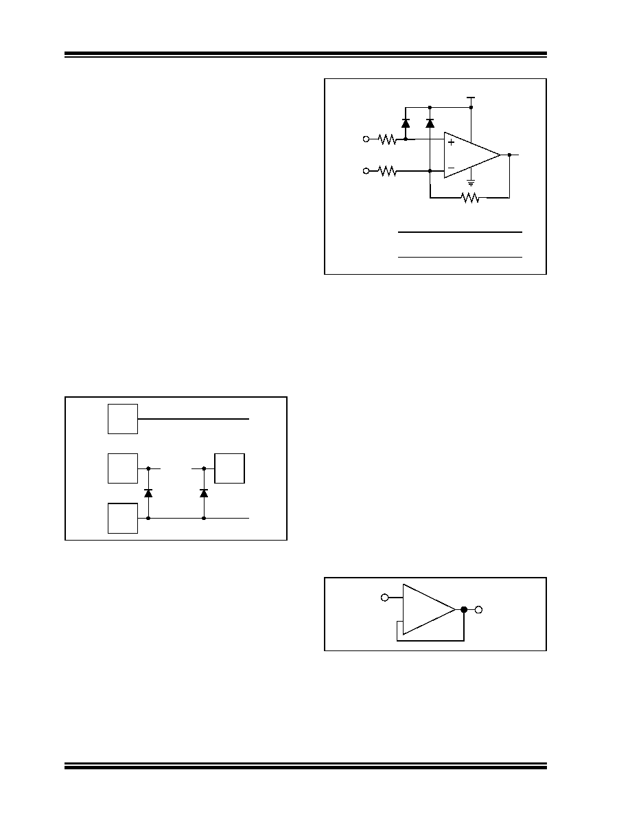
The ESD protection on the inputs can be depicted as
shown in Figure 4-1. This structure was chosen to
protect the input transistors, and to minimize input bias
current (IB). The input ESD diodes clamp the inputs
when they try to go more than one diode drop below
VSS. They also clamp any voltages that go too far
above VDD; their breakdown voltage is high enough to
allow normal operation, and low enough to bypass
quick ESD events within the specified limits.
FIGURE 4-1:
Simplified Analog Input ESD
Structures.
In order to prevent damage and/or improper operation
of these op amps, the circuit they are in must limit the
currents and voltages at the VIN+ and VIN– pins (see
Absolute Maximum Ratings at the beginning of
shows the recommended approach to protecting these
inputs. The internal ESD diodes prevent the input pins
(VIN+ and VIN–) from going too far below ground, and
the resistors R1 and R2 limit the possible current drawn
out of the input pins. Diodes D1 and D2 prevent the
input pins (VIN+ and VIN–) from going too far above
VDD, and dump any currents onto VDD. When
implemented as shown, resistors R1 and R2 also limit
the current through D1 and D2.
FIGURE 4-2:
Protecting the Analog
Inputs.
It is also possible to connect the diodes to the left of
resistors R1 and R2. In this case, current through the
diodes D1 and D2 needs to be limited by some other
mechanism. The resistors then serve as in-rush current
limiters; the DC current into the input pins (VIN+ and
VIN–) should be very small.
A significant amount of current can flow out of the
inputs when the common mode voltage (VCM) is below
high impedance may need to limit the useable voltage
range.
4.1.3
NORMAL OPERATION
The Common Mode Input Voltage Range (VCMR)
includes ground in single-supply systems (VSS), but
does not include VDD. This means that the amplifier
input behaves linearly as long as the Common Mode
Input Voltage (VCM) is kept within the specified VCMR
limits (VSS–0.3V to VDD–1.2V at +25°C).
same voltage as the inverting input, VOUT must be kept
below VDD–1.2V for correct operation.
FIGURE 4-3:
Unity Gain Buffer has a
Limited VOUT Range.
Bond
Pad
Bond
Pad
Bond
Pad
VDD
VIN+
VSS
Input
Stage
Bond
Pad
VIN–
V1
MCP60X
R1
VDD
D1
R1 >
VSS – (minimum expected V1)
2mA
R2 >
VSS – (minimum expected V2)
2mA
V2
R2
D2
R3
MCP60X
VOUT
+
–
VIN
相关PDF资料 |
PDF描述 |
|---|---|
| MCP602-I/SN | IC OPAMP DUAL SNGL SUPPLY 8SOIC |
| 1879011-1 | RES 220 OHM 2W 5% SMD |
| 1375870-5 | CONN RCPT 14POS VERT .8MM SMD |
| 4-1879011-7 | RES 18.0K OHM 2W 5% SMD |
| 87993-8 | CONN RCPT 8POS .156 VERT TIN |
相关代理商/技术参数 |
参数描述 |
|---|---|
| MCP602I-P | 制造商:MICROCHIP 制造商全称:Microchip Technology 功能描述:2.7V to 6.0V Single Supply CMOS Op Amps |
| MCP602-ISL | 制造商:MICROCHIP 制造商全称:Microchip Technology 功能描述:2.7V to 5.5V Single Supply CMOS Op Amps |
| MCP602-ISN | 制造商:MICROCHIP 制造商全称:Microchip Technology 功能描述:2.7V to 6.0V Single Supply CMOS Op Amps |
| MCP602-IST | 制造商:MICROCHIP 制造商全称:Microchip Technology 功能描述:2.7V to 5.5V Single Supply CMOS Op Amps |
| MCP602T | 制造商:MICROCHIP 制造商全称:Microchip Technology 功能描述:2.7V to 5.5V Single-Supply CMOS Op Amps |
发布紧急采购,3分钟左右您将得到回复。