参数资料
| 型号: | MCP6023-I/P |
| 厂商: | Microchip Technology |
| 文件页数: | 10/42页 |
| 文件大小: | 0K |
| 描述: | IC OPAMP 2.5V R-R I/O 8DIP |
| 标准包装: | 60 |
| 放大器类型: | 通用 |
| 电路数: | 1 |
| 输出类型: | 满摆幅 |
| 转换速率: | 7 V/µs |
| 增益带宽积: | 10MHz |
| 电流 - 输入偏压: | 1pA |
| 电压 - 输入偏移: | 500µV |
| 电流 - 电源: | 1mA |
| 电流 - 输出 / 通道: | 30mA |
| 电压 - 电源,单路/双路(±): | 2.5 V ~ 5.5 V |
| 工作温度: | -40°C ~ 85°C |
| 安装类型: | 通孔 |
| 封装/外壳: | 8-DIP(0.300",7.62mm) |
| 供应商设备封装: | 8-PDIP |
| 包装: | 管件 |
| 产品目录页面: | 679 (CN2011-ZH PDF) |
| 其它名称: | MCP6023I/P |
第1页第2页第3页第4页第5页第6页第7页第8页第9页当前第10页第11页第12页第13页第14页第15页第16页第17页第18页第19页第20页第21页第22页第23页第24页第25页第26页第27页第28页第29页第30页第31页第32页第33页第34页第35页第36页第37页第38页第39页第40页第41页第42页
MCP6021/1R/2/3/4
DS21685D-page 18
2009 Microchip Technology Inc.
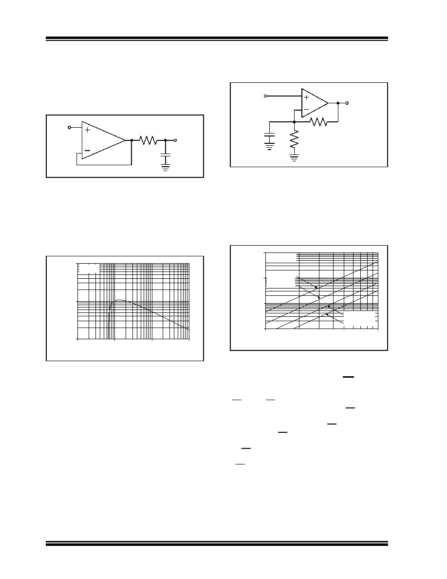
When driving large capacitive loads with these op
amps (e.g., > 60 pF when G = +1), a small series
feedback loop’s phase margin (stability) by making the
load resistive at higher frequencies. The bandwidth will
be generally lower than the bandwidth with no
capacitive load.
FIGURE 4-3:
Output Resistor RISO
Stabilizes Large Capacitive Loads.
different capacitive loads and gains. The x-axis is the
normalized load capacitance (CL/GN), where GN is the
circuit’s noise gain. For non-inverting gains, GN and the
Signal Gain are equal. For inverting gains, GN is
1+|Signal Gain| (e.g., -1 V/V gives GN = +2 V/V).
FIGURE 4-4:
Recommended RISO values
for capacitive loads.
After selecting RISO for your circuit, double-check the
resulting
frequency
response
peaking
and
step
response overshoot. Modify RISO’s value until the
response is reasonable. Evaluation on the bench and
simulations with the MCP6021/1R/2/3/4 Spice macro
model are helpful.
4.4
Gain Peaking
(frequency
response)
gain
peaking
and
(step
response) overshoot. The capacitance to ground at the
inverting input (CG) is the op amp’s common mode
input capacitance plus board parasitic capacitance. CG
is in parallel with RG, which causes an increase in gain
at high frequencies for non-inverting gains greater than
1 V/V (unity gain). CG also reduces the phase margin
of the feedback loop for both non-inverting and
inverting gains.
FIGURE 4-5:
Non-inverting Gain Circuit
with Parasitic Capacitance.
for various conditions. Other compensation techniques
may be used, but they tend to be more complicated to
the design.
FIGURE 4-6:
Non-inverting gain circuit
with parasitic capacitance.
4.5
MCP6023 Chip Select (CS)
The MCP6023 is a single amplifier with chip select
(CS). When CS is pulled high, the supply current drops
to 10 nA (typical) and flows through the CS pin to VSS.
When this happens, the amplifier output is put into a
high-impedance state. By pulling CS low, the amplifier
is enabled. The CS pin has an internal 5 M
Ω (typical)
pulldown resistor connected to VSS, so it will go low if
the CS pin is left floating. Figure 1-1 and Figure 2-39
show the output voltage and supply current response to
a CS pulse.
VIN
MCP602X
RISO
VOUT
CL
10
100
1,000
10
100
1,000
10,000
Normalized Capacitance; CL/GN (pF)
Recommended
R
IS
O
(
Ω
)
GN ≥ +1
VIN
RG
RF
VOUT
CG
1.E+02
1.E+03
1.E+04
1.E+05
110
Noise Gain; GN (V/V)
Maximum
R
F
(
Ω
)
GN > +1 V/V
100
1k
10k
100k
CG = 7 pF
CG = 20 pF
CG = 50 pF
CG = 100 pF
相关PDF资料 |
PDF描述 |
|---|---|
| TV02W140B-G | TVS 200W 14V BIDIRECT SOD-123 |
| 591621-4 | CONN 4MOD LGHTWGHT RAIL 74.96MM |
| TV02W131B-HF | TVS 200W 130V BIDIRECT SOD-123 |
| TV02W131B-G | TVS 200W 130V BIDIRECT SOD-123 |
| TLV342AIDG4 | IC OPAMP GP R-R 2.3MHZ 8SOIC |
相关代理商/技术参数 |
参数描述 |
|---|---|
| MCP6023T | 制造商:MICROCHIP 制造商全称:Microchip Technology 功能描述:Rail-to-Rail Input/Output, 10 MHz Op Amps |
| MCP6023T-E/MS | 制造商:MICROCHIP 制造商全称:Microchip Technology 功能描述:Rail-to-Rail Input/Output, 10 MHz Op Amps |
| MCP6023T-E/OT | 制造商:MICROCHIP 制造商全称:Microchip Technology 功能描述:Rail-to-Rail Input/Output, 10 MHz Op Amps |
| MCP6023T-E/P | 制造商:MICROCHIP 制造商全称:Microchip Technology 功能描述:Rail-to-Rail Input/Output, 10 MHz Op Amps |
| MCP6023T-E/SL | 制造商:MICROCHIP 制造商全称:Microchip Technology 功能描述:Rail-to-Rail Input/Output, 10 MHz Op Amps |
发布紧急采购,3分钟左右您将得到回复。