参数资料
| 型号: | MCP6031-E/MS |
| 厂商: | Microchip Technology |
| 文件页数: | 8/34页 |
| 文件大小: | 0K |
| 描述: | IC OPAMP SNGL 1.8V 8MSOP |
| 标准包装: | 100 |
| 放大器类型: | 通用 |
| 电路数: | 1 |
| 输出类型: | 满摆幅 |
| 转换速率: | 0.004 V/µs |
| 增益带宽积: | 10kHz |
| 电流 - 输入偏压: | 1pA |
| 电压 - 输入偏移: | 150µV |
| 电流 - 电源: | 0.9µA |
| 电流 - 输出 / 通道: | 23mA |
| 电压 - 电源,单路/双路(±): | 1.8 V ~ 5.5 V |
| 工作温度: | -40°C ~ 125°C |
| 安装类型: | 表面贴装 |
| 封装/外壳: | 8-TSSOP,8-MSOP(0.118",3.00mm 宽) |
| 供应商设备封装: | 8-MSOP |
| 包装: | 管件 |
| 产品目录页面: | 679 (CN2011-ZH PDF) |
| 配用: | MCP6031DM-PTPLS-ND - BOARD DEMO MCP6031 PHOTODIODE |
第1页第2页第3页第4页第5页第6页第7页当前第8页第9页第10页第11页第12页第13页第14页第15页第16页第17页第18页第19页第20页第21页第22页第23页第24页第25页第26页第27页第28页第29页第30页第31页第32页第33页第34页
MCP6031/2/3/4
DS22041B-page 16
2008 Microchip Technology Inc.
4.6
Supply Bypass
With this family of operational amplifiers, the power
supply pin (VDD for single-supply) should have a local
bypass capacitor (i.e., 0.01 F to 0.1 F) within 2 mm
for good high frequency performance. It can use a bulk
capacitor (i.e., 1 F or larger) within 100 mm to provide
large, slow currents. This bulk capacitor can be shared
with other analog parts.
4.7
Unused Op Amps
An unused op amp in a quad package (MCP6034)
should be configured as shown in Figure 4-5. These
circuits prevent the output from toggling and causing
crosstalk. Circuits A sets the op amp at its minimum
noise gain. The resistor divider produces any desired
reference voltage within the output voltage range of the
op amp; the op amp buffers that reference voltage.
Circuit B uses the minimum number of components
and operates as a comparator, but it may draw more
current.
FIGURE 4-5:
Unused Op Amps.
4.8
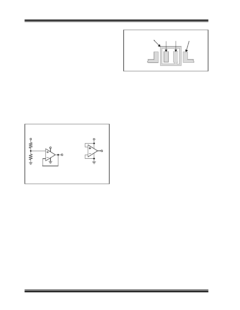
PCB Surface Leakage
In applications where low input bias current is critical,
Printed Circuit Board (PCB) surface leakage effects
need to be considered. Surface leakage is caused by
humidity, dust or other contamination on the board.
Under low humidity conditions, a typical resistance
between nearby traces is 1012
Ω. A 5V difference would
cause 5 pA of current to flow; which is greater than the
MCP6031/2/3/4
family’s
bias
current
at
+25°C
(±1.0 pA, typical).
The easiest way to reduce surface leakage is to use a
guard ring around sensitive pins (or traces). The guard
ring is biased at the same voltage as the sensitive pin.
An example of this type of layout is shown in
FIGURE 4-6:
Example Guard Ring Layout
for Inverting Gain.
1.
Non-inverting Gain and Unity-Gain Buffer:
a.
Connect the non-inverting pin (VIN+) to the
input with a wire that does not touch the
PCB surface.
b.
Connect the guard ring to the inverting input
pin (VIN–). This biases the guard ring to the
common mode input voltage.
2.
Inverting Gain and Transimpedance Gain Ampli-
fiers (convert current to voltage, such as photo
detectors):
a.
Connect the guard ring to the non-inverting
input pin (VIN+). This biases the guard ring
to the same reference voltage as the op
amp (e.g., VDD/2 or ground).
b.
Connect the inverting pin (VIN–) to the input
with a wire that does not touch the PCB
surface.
VDD
MCP6034 (A)
MCP6034 (B)
R1
R2
VDD
VREF
V
REF
V
DD
R
2
R
1
R
2
+
------------------
=
Guard Ring
VIN–VIN+
VSS
相关PDF资料 |
PDF描述 |
|---|---|
| MCP608T-I/ST | IC OPAMP 2.5V R-R W/CS 8TSSOP |
| MCP6232-E/SN | IC OPAMP 1.8V DUAL R-R 8SOIC |
| MCP629T-E/ML | IC OPAMP GP RR 20MHZ W/CS 16QFN |
| MCP639-E/ML | IC OP AMP QUAD 24MHZ 16-QFN |
| MCP6409T-H/SL | IC OPAMP QUAD 1.8V 1MHZ 14SOIC |
相关代理商/技术参数 |
参数描述 |
|---|---|
| MCP6031T | 制造商:MICROCHIP 制造商全称:Microchip Technology 功能描述:0.9 uA, High Precision Op Amps |
| MCP6031T-E/MC | 功能描述:运算放大器 - 运放 SNGL 18V 10kHz Op Amp E Temp RoHS:否 制造商:STMicroelectronics 通道数量:4 共模抑制比(最小值):63 dB 输入补偿电压:1 mV 输入偏流(最大值):10 pA 工作电源电压:2.7 V to 5.5 V 安装风格:SMD/SMT 封装 / 箱体:QFN-16 转换速度:0.89 V/us 关闭:No 输出电流:55 mA 最大工作温度:+ 125 C 封装:Reel |
| MCP6031TE/MS | 制造商:MICROCHIP 制造商全称:Microchip Technology 功能描述:0.9 uA, High Precision Op Amps |
| MCP6031T-E/MS | 功能描述:运算放大器 - 运放 S-1.8V 14kHz Op Amp E temp RoHS:否 制造商:STMicroelectronics 通道数量:4 共模抑制比(最小值):63 dB 输入补偿电压:1 mV 输入偏流(最大值):10 pA 工作电源电压:2.7 V to 5.5 V 安装风格:SMD/SMT 封装 / 箱体:QFN-16 转换速度:0.89 V/us 关闭:No 输出电流:55 mA 最大工作温度:+ 125 C 封装:Reel |
| MCP6031T-E/OT | 功能描述:运算放大器 - 运放 SNGL 1.8V 10kHz Op Amp E Temp RoHS:否 制造商:STMicroelectronics 通道数量:4 共模抑制比(最小值):63 dB 输入补偿电压:1 mV 输入偏流(最大值):10 pA 工作电源电压:2.7 V to 5.5 V 安装风格:SMD/SMT 封装 / 箱体:QFN-16 转换速度:0.89 V/us 关闭:No 输出电流:55 mA 最大工作温度:+ 125 C 封装:Reel |
发布紧急采购,3分钟左右您将得到回复。