- 您现在的位置:买卖IC网 > PDF目录16755 > MCP6031DM-PTPLS (Microchip Technology)BOARD DEMO MCP6031 PHOTODIODE PDF资料下载
参数资料
| 型号: | MCP6031DM-PTPLS |
| 厂商: | Microchip Technology |
| 文件页数: | 7/34页 |
| 文件大小: | 0K |
| 描述: | BOARD DEMO MCP6031 PHOTODIODE |
| 标准包装: | 1 |
| 系列: | PICtail™ Plus |
| 主要目的: | 接口,传感器至模数转换器接口,光电检测器 |
| 嵌入式: | 否 |
| 已用 IC / 零件: | MCP6031 |
| 主要属性: | 光电流至电压转换 |
| 次要属性: | RC 低通滤波器 |
| 已供物品: | 板,CD |
| 产品目录页面: | 681 (CN2011-ZH PDF) |
| 相关产品: | MCP6031T-E/OTDKR-ND - IC OPAMP SNGL 1.8V SOT23-5 MCP6031T-E/OTCT-ND - IC OPAMP SNGL 1.8V SOT23-5 MCP6031T-E/MCTR-ND - IC OPAMP SNGL 1.8V 8DFN MCP6031-E/MC-ND - IC OPAMP SNGL 1.8V 8DFN MCP6031-E/MS-ND - IC OPAMP SNGL 1.8V 8MSOP MCP6031-E/SN-ND - IC OPAMP SNGL 1.8V 8SOIC MCP6031T-E/MSTR-ND - IC OPAMP SNGL 1.8V 8MSOP MCP6031T-E/SNTR-ND - IC OPAMP SNGL 1.8V 8SOIC MCP6031T-E/OTTR-ND - IC OPAMP SNGL 1.8V SOT23-5 |
第1页第2页第3页第4页第5页第6页当前第7页第8页第9页第10页第11页第12页第13页第14页第15页第16页第17页第18页第19页第20页第21页第22页第23页第24页第25页第26页第27页第28页第29页第30页第31页第32页第33页第34页
2008 Microchip Technology Inc.
DS22041B-page 15
MCP6031/2/3/4
4.2
Rail-to-Rail Output
The output voltage range of the MCP6031/2/3/4 op
amps is VSS + 10 mV (minimum) and VDD – 10 mV
(maximum) when RL =50kΩ is connected to VDD/2
more information.
4.3
Output Loads and Battery Life
The MCP6031/2/3/4 op amp family has outstanding
quiescent current, which supports battery-powered
applications. There is minimal quiescent current glitch-
ing when Chip Select (CS) is raised or lowered. This
prevents excessive current draw, and reduced battery
life, when the part is turned off or on.
Heavy resistive loads at the output can cause exces-
sive battery drain. Driving a DC voltage of 2.5V across
a 100 k
Ω load resistor will cause the supply current to
increase by 25 A, depleting the battery 28 times as
fast as IQ (0.9 A, typical) alone.
High frequency signals (fast edge rate) across capaci-
tive loads will also significantly increase supply current.
For instance, a 0.1 F capacitor at the output presents
an AC impedance of 15.9 k
Ω (1/2πfC) to a 100 Hz
sinewave. It can be shown that the average power
drawn from the battery by a 5.0 Vp-p sinewave
(1.77 Vrms), under these conditions, is
EQUATION 4-1:
This will drain the battery about 12 times as fast as IQ
alone.
4.4
Capacitive Loads
Driving large capacitive loads can cause stability
problems for voltage feedback op amps. As the load
capacitance increases, the feedback loop’s phase
margin decreases and the closed-loop bandwidth is
reduced. This produces gain peaking in the frequency
response, with overshoot and ringing in the step
response. While a unity-gain buffer (G = +1) is the most
sensitive to capacitive loads, all gains show the same
general behavior.
When driving large capacitive loads with these op
amps (e.g., > 100 pF when G = +1), a small series
feedback loop’s phase margin (stability) by making the
output load resistive at higher frequencies. The
bandwidth will be generally lower than the bandwidth
with no capacitance load.
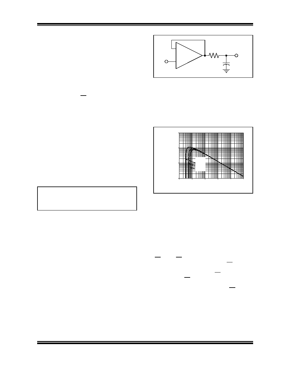
FIGURE 4-3:
Output resistor, RISO
stabilizes large capacitive loads.
different capacitive loads and gains. The x-axis is the
normalized load capacitance (CL/GN), where GN is the
circuit's noise gain. For non-inverting gains, GN and the
Signal Gain are equal. For inverting gains, GN is
1+|Signal Gain| (e.g., -1 V/V gives GN = +2 V/V).
FIGURE 4-4:
Recommended RISO values
for Capacitive Loads.
After selecting RISO for your circuit, double-check the
resulting
frequency
response
peaking
and
step
response overshoot. Modify RISO’s value until the
response is reasonable. Bench evaluation and simula-
tions with the MCP6031/2/3/4 SPICE macro model are
very helpful.
4.5
MCP6033 Chip Select
The MCP6033 is a single op amp with Chip Select
(CS). When CS is pulled high, the supply current drops
to 0.4 nA (typical) and flows through the CS pin to VSS.
When this happens, the amplifier output is put into a
high impedance state. By pulling CS low, the amplifier
is enabled. If the CS pin is left floating, the amplifier will
not operate properly. Figure 1-1 shows the output
voltage and supply current response to a CS pulse.
PSupply = (VDD - VSS) (IQ + VL(p-p) f CL )
= (5V)(0.9 A + 5.0Vp-p 100Hz 0.1F)
= 4.5 W + 50 W
VIN
RISO
VOUT
MCP603X
CL
–
+
1000
10000
100000
1000000
1.E-11 1.E-10 1.E-09 1.E-08 1.E-07 1.E-06
Normalized Load Capacitance; CL/GN (F)
Re
co
m
ende
d
R
IS
O
(
)
GN:
1 V/V
2 V/V
≥ 5 V/V
10p
100p
1n
10n
100n
1
1M
100k
10k
1k
相关PDF资料 |
PDF描述 |
|---|---|
| V300B36E150BG2 | CONVERTER MOD DC/DC 36V 150W |
| V48C8E150BL3 | CONVERTER MOD DC/DC 8V 150W |
| ADM00313 | BOARD EVAL LI-ION CHRG MCP73830L |
| V48C8E150BL | CONVERTER MOD DC/DC 8V 150W |
| H8PPH-1618M | DIP CABLE - HDP16H/AE16M/HDP16H |
相关代理商/技术参数 |
参数描述 |
|---|---|
| MCP6031DM-PTPLS | 制造商:Microchip Technology Inc 功能描述:Operational Amplifier Demo Board |
| MCP6031-E/MC | 功能描述:运算放大器 - 运放 SNGL 18V 10kHz Op Amp E Temp RoHS:否 制造商:STMicroelectronics 通道数量:4 共模抑制比(最小值):63 dB 输入补偿电压:1 mV 输入偏流(最大值):10 pA 工作电源电压:2.7 V to 5.5 V 安装风格:SMD/SMT 封装 / 箱体:QFN-16 转换速度:0.89 V/us 关闭:No 输出电流:55 mA 最大工作温度:+ 125 C 封装:Reel |
| MCP6031E/MS | 制造商:MICROCHIP 制造商全称:Microchip Technology 功能描述:0.9 uA, High Precision Op Amps |
| MCP6031-E/MS | 功能描述:运算放大器 - 运放 S-1.8V 14kHz Op Amp E temp RoHS:否 制造商:STMicroelectronics 通道数量:4 共模抑制比(最小值):63 dB 输入补偿电压:1 mV 输入偏流(最大值):10 pA 工作电源电压:2.7 V to 5.5 V 安装风格:SMD/SMT 封装 / 箱体:QFN-16 转换速度:0.89 V/us 关闭:No 输出电流:55 mA 最大工作温度:+ 125 C 封装:Reel |
| MCP6031-E/OT | 制造商:MICROCHIP 制造商全称:Microchip Technology 功能描述:0.9 μA, High Precision Op Amps |
发布紧急采购,3分钟左右您将得到回复。