- 您现在的位置:买卖IC网 > PDF目录5726 > MCP6033T-E/MS (Microchip Technology)IC OPAMP SNGL 1.8V W/CS 8MSOP PDF资料下载
参数资料
| 型号: | MCP6033T-E/MS |
| 厂商: | Microchip Technology |
| 文件页数: | 6/34页 |
| 文件大小: | 0K |
| 描述: | IC OPAMP SNGL 1.8V W/CS 8MSOP |
| 标准包装: | 2,500 |
| 放大器类型: | 通用 |
| 电路数: | 1 |
| 输出类型: | 满摆幅 |
| 转换速率: | 0.004 V/µs |
| 增益带宽积: | 10kHz |
| 电流 - 输入偏压: | 1pA |
| 电压 - 输入偏移: | 150µV |
| 电流 - 电源: | 0.9µA |
| 电流 - 输出 / 通道: | 23mA |
| 电压 - 电源,单路/双路(±): | 1.8 V ~ 5.5 V |
| 工作温度: | -40°C ~ 125°C |
| 安装类型: | 表面贴装 |
| 封装/外壳: | 8-TSSOP,8-MSOP(0.118",3.00mm 宽) |
| 供应商设备封装: | 8-MSOP |
| 包装: | 带卷 (TR) |
| 其它名称: | MCP6033T-E/MSTR |
第1页第2页第3页第4页第5页当前第6页第7页第8页第9页第10页第11页第12页第13页第14页第15页第16页第17页第18页第19页第20页第21页第22页第23页第24页第25页第26页第27页第28页第29页第30页第31页第32页第33页第34页
MCP6031/2/3/4
DS22041B-page 14
2008 Microchip Technology Inc.
4.0
APPLICATION INFORMATION
The MCP6031/2/3/4 family of op amps is manufactured
using Microchip’s state-of-the-art CMOS process and
is specifically designed for low-power, high precision
applications.
4.1
Rail-to-Rail Input
4.1.1
PHASE REVERASAL
The MCP6031/2/3/4 op amps are designed to prevent
phase reversal when the input pins exceed the supply
voltages. Figure 2-32 shows the input voltage exceed-
ing the supply voltage without any phase reversal.
4.1.2
INPUT VOLTAGE AND CURRENT
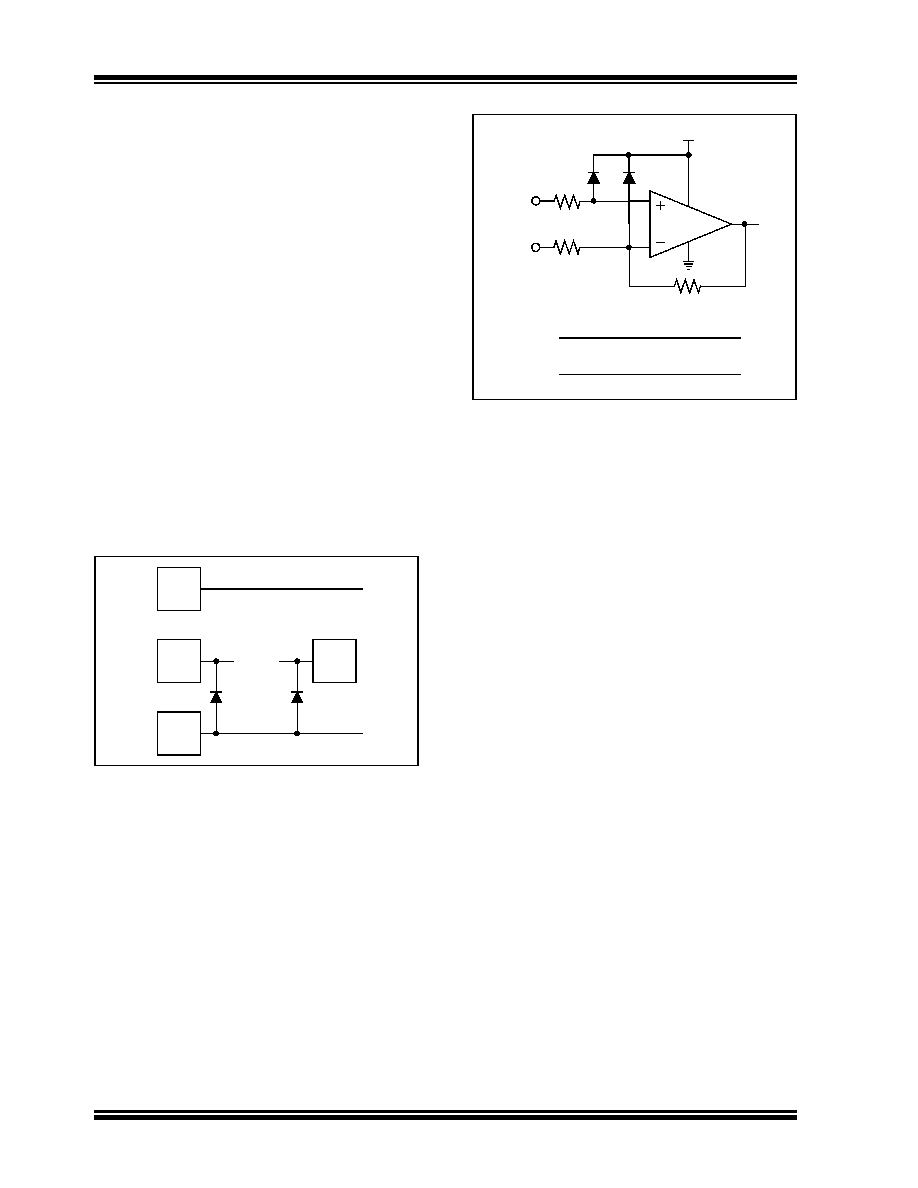
LIMITS
The ESD protection on the inputs can be depicted as
shown in Figure 4-1. This structure was chosen to
protect the input transistors and to minimize input bias
current (IB). The input ESD diodes clamp the inputs
when they try to go more than one diode drop below
VSS. They also clamp any voltage that go too far above
VDD; their breakdown voltage is high enough to allow
normal operation and low enough to bypass ESD
events within the specified limits.
FIGURE 4-1:
Simplified Analog Input ESD
Structures.
In order to prevent damage and/or improper operation
of these op amps, the circuit they are in must limit the
voltages and currents at the VIN+ and VIN- pins (see
Absolute Maximum Ratings at the beginning of
shows the recommended approach to protecting these
inputs. The internal ESD diodes prevent the input pins
(VIN+ and VIN-) from going too far below ground, and
the resistors R1 and R2 limit the possible current drawn
out of the input pins. Diodes D1 and D2 prevent the
input pins (VIN+ and VIN-) from going too far above VDD.
When implemented as shown, resistors R1 and R2 also
limit the current through D1 and D2.
FIGURE 4-2:
Protecting the Analog
Inputs.
It is also possible to connect the diodes to the left of the
resistors R1 and R2. In this case, the currents through
the diodes D1 and D2 need to be limited by some other
mechanism. The resistors then serve as in-rush current
limiters; the DC currents into the input pins (VIN+ and
VIN-) should be very small. A significant amount of
current can flow out of the inputs when the common
mode voltage (VCM) is below ground (VSS).
4.1.3
NORMAL OPERATION
The input stage of the MCP6031/2/3/4 op amps uses
two differential input stages in parallel. One operates at
a low common mode input voltage (VCM), while the
other operates at a high VCM. With this topology, the
device operates with a VCM up to 300 mV above VDD
and 300 mV below VSS. The input offset voltage is
measured at VCM = VSS – 0.3V and VDD + 0.3V to
ensure proper operation.
There are two transitions in input behavior as VCM is
changed. The first occurs, when VCM is near
VSS + 0.4V, and the second occurs when VCM is near
VDD – 0.5V. For the best distortion performance with
non-inverting gains, avoid these regions of operation.
Bond
Pad
Bond
Pad
Bond
Pad
VDD
VIN+
VSS
Input
Stage
Bond
Pad
VIN–
V1
MCP603X
R1
VDD
D1
R1 >
VSS – (minimum expected V1)
2mA
R2 >
VSS – (minimum expected V2)
2mA
V2
R2
D2
R3
相关PDF资料 |
PDF描述 |
|---|---|
| LT1127ACN | IC OP-AMP DECOMPENSAT QUAD 14DIP |
| 2036-47-C3 | GAS DISCHARGE TUBE MINI 3 POLE |
| 180901 | CONN HOUSING RCPT 4POS FASTON |
| 360010-1 | CONN RECEPT FASTON 3CIR .187 |
| 77313-122-44LF | CONN HEADER .100 DUAL STR 44POS |
相关代理商/技术参数 |
参数描述 |
|---|---|
| MCP6034 | 制造商:MICROCHIP 制造商全称:Microchip Technology 功能描述:0.9 uA, High Precision Op Amps |
| MCP6034-E/MC | 制造商:MICROCHIP 制造商全称:Microchip Technology 功能描述:0.9 μA, High Precision Op Amps |
| MCP6034E/MS | 制造商:MICROCHIP 制造商全称:Microchip Technology 功能描述:0.9 uA, High Precision Op Amps |
| MCP6034-E/MS | 制造商:MICROCHIP 制造商全称:Microchip Technology 功能描述:0.9 μA, High Precision Op Amps |
| MCP6034-E/OT | 制造商:MICROCHIP 制造商全称:Microchip Technology 功能描述:0.9 μA, High Precision Op Amps |
发布紧急采购,3分钟左右您将得到回复。