- 您现在的位置:买卖IC网 > PDF目录3746 > MCP623T-E/CHY (Microchip Technology)IC OPAMP SGL 2.5MA 20MHZ SOT23-6 PDF资料下载
参数资料
| 型号: | MCP623T-E/CHY |
| 厂商: | Microchip Technology |
| 文件页数: | 20/66页 |
| 文件大小: | 0K |
| 描述: | IC OPAMP SGL 2.5MA 20MHZ SOT23-6 |
| 标准包装: | 1 |
| 系列: | mCal 技术 |
| 放大器类型: | 通用 |
| 电路数: | 1 |
| 输出类型: | 满摆幅 |
| 转换速率: | 10 V/µs |
| 增益带宽积: | 20MHz |
| 电流 - 输入偏压: | 5pA |
| 电压 - 输入偏移: | 200µV |
| 电流 - 电源: | 2.5mA |
| 电流 - 输出 / 通道: | 70mA |
| 电压 - 电源,单路/双路(±): | 2.5 V ~ 5.5 V |
| 工作温度: | -40°C ~ 125°C |
| 安装类型: | 表面贴装 |
| 封装/外壳: | SOT-23-6 |
| 供应商设备封装: | SOT-23-6 |
| 包装: | 标准包装 |
| 其它名称: | MCP623T-E/CHYDKR |
第1页第2页第3页第4页第5页第6页第7页第8页第9页第10页第11页第12页第13页第14页第15页第16页第17页第18页第19页当前第20页第21页第22页第23页第24页第25页第26页第27页第28页第29页第30页第31页第32页第33页第34页第35页第36页第37页第38页第39页第40页第41页第42页第43页第44页第45页第46页第47页第48页第49页第50页第51页第52页第53页第54页第55页第56页第57页第58页第59页第60页第61页第62页第63页第64页第65页第66页
2009-2011 Microchip Technology Inc.
DS22188C-page 27
MCP621/1S/2/3/4/5/9
4.4
Improving Stability
4.4.1
CAPACITIVE LOADS
Driving large capacitive loads can cause stability
problems for voltage feedback op amps. As the load
capacitance increases, the feedback loop’s phase
margin decreases and the closed-loop bandwidth is
reduced. This produces gain peaking in the frequency
response, with overshoot and ringing in the step
response. See Figure 2-30. A unity gain buffer (G = +1)
is the most sensitive to capacitive loads, though all
gains show the same general behavior.
When driving large capacitive loads with these op
amps (e.g., > 10 pF when G = +1), a small series
feedback loop’s phase margin (stability) by making the
output load resistive at higher frequencies. The
bandwidth will be generally lower than the bandwidth
with no capacitive load.
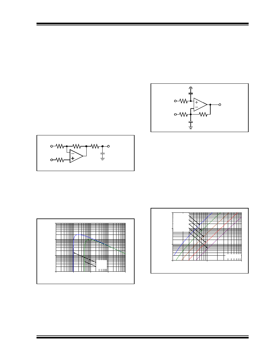
FIGURE 4-9:
Output Resistor, RISO
Stabilizes Large Capacitive Loads.
different capacitive loads and gains. The x-axis is the
normalized load capacitance (CL/GN), where GN is the
circuit’s noise gain. For non-inverting gains, GN and the
Signal Gain are equal. For inverting gains, GN is
1+|Signal Gain| (e.g., -1 V/V gives GN =+2V/V).
FIGURE 4-10:
Recommended RISO Values
for Capacitive Loads.
After selecting RISO for your circuit, double check the
resulting frequency response peaking and step
response overshoot. Modify RISO’s value until the
response is reasonable. Bench evaluation and
simulations with the MCP621/1S/2/3/4/5/9 SPICE
macro model are helpful.
4.4.2
GAIN PEAKING
Figure 4-11 shows an op amp circuit that represents
non-inverting amplifiers (VM is a DC voltage and VP is
the input) or inverting amplifiers (VP is a DC voltage
and VM is the input). The capacitances CN and CG
represent the total capacitance at the input pins; they
include the op amp’s Common mode input capacitance
(CCM), board parasitic capacitance and any capacitor
placed in parallel.
FIGURE 4-11:
Amplifier with Parasitic
Capacitance.
CG acts in parallel with RG (except for a gain of +1 V/V),
which causes an increase in gain at high frequencies.
CG also reduces the phase margin of the feedback
loop, which becomes less stable. This effect can be
reduced by either reducing CG or RF.
CN and RN form a low-pass filter that affects the signal
at VP. This filter has a single real pole at 1/(2πRNCN).
The largest value of RF that should be used depends
recommended RF for several CG values.
FIGURE 4-12:
Maximum Recommended
RF vs. Gain.
signal step responses at G = +1 V/V. The unity gain
buffer usually has RF =0Ω and RG open.
signal step responses at G = -1 V/V. Since the noise
gain is 2 V/V and CG ≈ 10 pF, the resistors were
chosen to be RF =RG =1kΩ and RN =500Ω.
RISO
VOUT
CL
RG
RF
RN
MCP62X
1
10
100
1,000
1.E-12
1.E-11
1.E-10
1.E-09
1.E-08
Normalized Capacitance; CL/GN (F)
R
ec
o
m
en
de
d
R
IS
O
(
)
GN = +1
GN ≥ +2
1p
100p
1n
10n
10p
VP
RF
VOUT
RN
CN
VM
RG
CG
MCP62X
1.E+02
1.E+03
1.E+04
1.E+05
110
100
Noise Gain; GN (V/V)
M
axi
m
u
m
R
eco
m
en
ded
R
F
(
)
GN > +1 V/V
100
10k
100k
1k
CG = 10 pF
CG = 32 pF
CG = 100 pF
CG = 320 pF
CG = 1 nF
相关PDF资料 |
PDF描述 |
|---|---|
| 960208-6303-AR | CONN SOCKET DUAL VERT 8POS GOLD |
| 960110-6202-AR | CONN SOCKET SGL VERT 10POS GOLD |
| 150208-2000-TH | CONN SOCKET 2MM 8POS SMD 15GOLD |
| MCP621ST-E/OT | IC OPAMP SGL 2.5MA 20MHZ SOT23-5 |
| 929870-01-04-10 | CONN RCPT 4POS STR .100" GOLD |
相关代理商/技术参数 |
参数描述 |
|---|---|
| MCP6241-E/MC | 功能描述:运算放大器 - 运放 Single 1.8V 550 kHz OP E Temp RoHS:否 制造商:STMicroelectronics 通道数量:4 共模抑制比(最小值):63 dB 输入补偿电压:1 mV 输入偏流(最大值):10 pA 工作电源电压:2.7 V to 5.5 V 安装风格:SMD/SMT 封装 / 箱体:QFN-16 转换速度:0.89 V/us 关闭:No 输出电流:55 mA 最大工作温度:+ 125 C 封装:Reel |
| MCP6241-E/MS | 功能描述:运算放大器 - 运放 Single 1.8V 500KHz RoHS:否 制造商:STMicroelectronics 通道数量:4 共模抑制比(最小值):63 dB 输入补偿电压:1 mV 输入偏流(最大值):10 pA 工作电源电压:2.7 V to 5.5 V 安装风格:SMD/SMT 封装 / 箱体:QFN-16 转换速度:0.89 V/us 关闭:No 输出电流:55 mA 最大工作温度:+ 125 C 封装:Reel |
| MCP6241-E/MS | 制造商:Microchip Technology Inc 功能描述:; LEADED PROCESS COMPATIBLE:YES; PEAK RE |
| MCP6241-E/P | 功能描述:运算放大器 - 运放 Single 1.8V 500KHz RoHS:否 制造商:STMicroelectronics 通道数量:4 共模抑制比(最小值):63 dB 输入补偿电压:1 mV 输入偏流(最大值):10 pA 工作电源电压:2.7 V to 5.5 V 安装风格:SMD/SMT 封装 / 箱体:QFN-16 转换速度:0.89 V/us 关闭:No 输出电流:55 mA 最大工作温度:+ 125 C 封装:Reel |
| MCP6241-E/SN | 功能描述:运算放大器 - 运放 Single 1.8V 500KHz RoHS:否 制造商:STMicroelectronics 通道数量:4 共模抑制比(最小值):63 dB 输入补偿电压:1 mV 输入偏流(最大值):10 pA 工作电源电压:2.7 V to 5.5 V 安装风格:SMD/SMT 封装 / 箱体:QFN-16 转换速度:0.89 V/us 关闭:No 输出电流:55 mA 最大工作温度:+ 125 C 封装:Reel |
发布紧急采购,3分钟左右您将得到回复。