参数资料
| 型号: | MCP6442-E/MS |
| 厂商: | Microchip Technology |
| 文件页数: | 6/46页 |
| 文件大小: | 0K |
| 描述: | IC OPAMP DUAL 1.6V 9KHZ 8MSOP |
| 标准包装: | 100 |
| 放大器类型: | 通用 |
| 电路数: | 2 |
| 输出类型: | 满摆幅 |
| 转换速率: | 0.003 V/µs |
| 增益带宽积: | 9kHz |
| 电流 - 输入偏压: | 1pA |
| 电压 - 输入偏移: | 4500µV |
| 电流 - 电源: | 0.45µA |
| 电流 - 输出 / 通道: | 22mA |
| 电压 - 电源,单路/双路(±): | 1.4 V ~ 6 V |
| 工作温度: | -40°C ~ 125°C |
| 安装类型: | 表面贴装 |
| 封装/外壳: | 8-TSSOP,8-MSOP(0.118",3.00mm 宽) |
| 供应商设备封装: | 8-MSOP |
| 包装: | 管件 |
第1页第2页第3页第4页第5页当前第6页第7页第8页第9页第10页第11页第12页第13页第14页第15页第16页第17页第18页第19页第20页第21页第22页第23页第24页第25页第26页第27页第28页第29页第30页第31页第32页第33页第34页第35页第36页第37页第38页第39页第40页第41页第42页第43页第44页第45页第46页
MCP6441/2/4
DS22257C-page 14
2010-2012 Microchip Technology Inc.
4.1.4
NORMAL OPERATION
The input stage of the MCP6441/2/4 op amp uses two
differential input stages in parallel. One operates at a
low Common Mode input voltage (VCM), while the other
operates at a high VCM. With this topology, the device
operates with a VCM up to 300 mV above VDD and
300 mV below VSS. The input offset voltage is
measured at VCM =VSS – 0.3V and VDD + 0.3V, to
ensure proper operation.
The transition between the input stages occurs when
the best distortion performance and gain linearity, with
non-inverting gains, avoid this region of operation.
4.2
Rail-to-Rail Output
The output voltage range of the MCP6441/2/4 op amp
is VSS + 20 mV (minimum) and VDD – 20 mV (maxi-
mum) when RL =10kΩ is connected to VDD/2 and
information.
4.3
Capacitive Loads
Driving large capacitive loads can cause stability
problems for voltage feedback op amps. As the load
capacitance increases, the feedback loop’s phase
margin decreases, and the closed-loop bandwidth is
reduced. This produces gain peaking in the frequency
response, with overshoot and ringing in the step
response. While a unity-gain buffer (G = +1 V/V) is the
most sensitive to the capacitive loads, all gains show
the same general behavior.
When
driving
large
capacitive
loads
with
the
MCP6441/2/4
op
amp
(e.g.,
> 100 pF
when
G = +1 V/V), a small series resistor at the output (RISO
in Figure 4-4) improves the feedback loop’s phase mar-
gin (stability) by making the output load resistive at
higher frequencies. The bandwidth will be generally
lower than the bandwidth with no capacitance load.
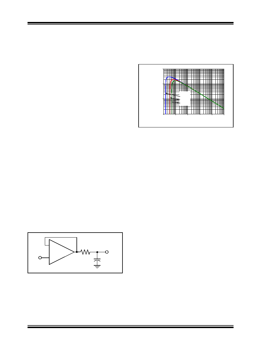
FIGURE 4-4:
Output Resistor, RISO
Stabilizes Large Capacitive Loads.
different capacitive loads and gains. The x-axis is the
normalized load capacitance (CL/GN), where GN is the
circuit's noise gain. For non-inverting gains, GN and the
Signal Gain are equal. For inverting gains, GN is
1+|Signal Gain| (e.g., -1 V/V gives GN = +2 V/V).
FIGURE 4-5:
Recommended RISO Values
for Capacitive Loads.
After selecting RISO for your circuit, double-check the
resulting
frequency
response
peaking
and
step
response overshoot. Modify RISO’s value until the
response
is
reasonable.
Bench
evaluation
and
simulations with the MCP6441/2/4 SPICE macro
model are very helpful.
4.4
Supply Bypass
The MCP6441/2/4 op amp’s power supply pin (VDD for
single-supply) should have a local bypass capacitor
(i.e., 0.01 F to 0.1 F) within 2 mm for good high
frequency performance. It can use a bulk capacitor
(i.e., 1 F or larger) within 100 mm to provide large,
slow currents. This bulk capacitor can be shared with
other analog parts.
4.5
PCB Surface Leakage
In applications where low input bias current is critical,
Printed Circuit Board (PCB) surface leakage effects
need to be considered. Surface leakage is caused by
humidity, dust or other contamination on the board.
Under low humidity conditions, a typical resistance
between nearby traces is 1012
Ω. A 5V difference would
cause 5 pA of current to flow, which is greater than the
MCP6441/2/4 op amp’s bias current at +25°C (±1 pA,
typical).
VIN
RISO
VOUT
CL
–
+
MCP644X
1000
10000
100000
1000000
1.E-11 1.E-10 1.E-09 1.E-08 1.E-07 1.E-06
Normalized Load Capacitance; CL/GN (F)
Re
c
o
m
en
d
ed
R
IS
O
(
)
GN:
1 V/V
2 V/V
≥ 5 V/V
10p
100p
1n
10n
0.1
1
1k
10k
100k
1M
相关PDF资料 |
PDF描述 |
|---|---|
| MCP659T-E/ML | IC OP AMP 50MHZ RRIO 16QFN |
| MCP662-E/MS | IC OP AMP 60MHZ DUAL 8-MSOP |
| MCP669T-E/ML | IC OPAMP QUAD 60MHZ 16QFN |
| MCP6H04T-E/SL | IC OPAMP QUAD16V 1.2MHZ 14SOIC |
| MCP6N11T-100E/SN | IC AMP INSTR RRIO 35MHZ 8SOIC |
相关代理商/技术参数 |
参数描述 |
|---|---|
| MCP6442T-E/MNY | 功能描述:运算放大器 - 运放 450 nA, 9 kHz Op Amp RoHS:否 制造商:STMicroelectronics 通道数量:4 共模抑制比(最小值):63 dB 输入补偿电压:1 mV 输入偏流(最大值):10 pA 工作电源电压:2.7 V to 5.5 V 安装风格:SMD/SMT 封装 / 箱体:QFN-16 转换速度:0.89 V/us 关闭:No 输出电流:55 mA 最大工作温度:+ 125 C 封装:Reel |
| MCP6442T-E/MS | 功能描述:运算放大器 - 运放 450 nA, 9 kHz Op Amp RoHS:否 制造商:STMicroelectronics 通道数量:4 共模抑制比(最小值):63 dB 输入补偿电压:1 mV 输入偏流(最大值):10 pA 工作电源电压:2.7 V to 5.5 V 安装风格:SMD/SMT 封装 / 箱体:QFN-16 转换速度:0.89 V/us 关闭:No 输出电流:55 mA 最大工作温度:+ 125 C 封装:Reel |
| MCP6442T-E/SN | 功能描述:运算放大器 - 运放 450 nA, 9 kHz Op Amp RoHS:否 制造商:STMicroelectronics 通道数量:4 共模抑制比(最小值):63 dB 输入补偿电压:1 mV 输入偏流(最大值):10 pA 工作电源电压:2.7 V to 5.5 V 安装风格:SMD/SMT 封装 / 箱体:QFN-16 转换速度:0.89 V/us 关闭:No 输出电流:55 mA 最大工作温度:+ 125 C 封装:Reel |
| MCP6444-E/SL | 功能描述:运算放大器 - 运放 450 nA, 9 kHz Op Amp RoHS:否 制造商:STMicroelectronics 通道数量:4 共模抑制比(最小值):63 dB 输入补偿电压:1 mV 输入偏流(最大值):10 pA 工作电源电压:2.7 V to 5.5 V 安装风格:SMD/SMT 封装 / 箱体:QFN-16 转换速度:0.89 V/us 关闭:No 输出电流:55 mA 最大工作温度:+ 125 C 封装:Reel |
| MCP6444-E/SL | 制造商:Microchip Technology Inc 功能描述:; Peak Reflow Compatible (260 C):Yes; Le 制造商:Microchip Technology Inc 功能描述:IC, OP-AMP |
发布紧急采购,3分钟左右您将得到回复。