参数资料
| 型号: | MCP6V27-E/MD |
| 厂商: | Microchip Technology |
| 文件页数: | 15/50页 |
| 文件大小: | 0K |
| 描述: | IC OPAMP DUAL AUTO-ZERO 8DFN |
| 标准包装: | 91 |
| 放大器类型: | 自动调零 |
| 电路数: | 2 |
| 输出类型: | 满摆幅 |
| 转换速率: | 1 V/µs |
| 增益带宽积: | 2MHz |
| 电流 - 输入偏压: | 7pA |
| 电压 - 输入偏移: | 2µV |
| 电流 - 电源: | 620µA |
| 电流 - 输出 / 通道: | 22mA |
| 电压 - 电源,单路/双路(±): | 2.3 V ~ 5.5 V |
| 工作温度: | -40°C ~ 125°C |
| 安装类型: | 表面贴装 |
| 封装/外壳: | 8-VDFN 裸露焊盘 |
| 供应商设备封装: | 8-DFN(4x4) |
| 包装: | 管件 |
第1页第2页第3页第4页第5页第6页第7页第8页第9页第10页第11页第12页第13页第14页当前第15页第16页第17页第18页第19页第20页第21页第22页第23页第24页第25页第26页第27页第28页第29页第30页第31页第32页第33页第34页第35页第36页第37页第38页第39页第40页第41页第42页第43页第44页第45页第46页第47页第48页第49页第50页
MCP6V26/7/8
DS25007B-page 22
2011 Microchip Technology Inc.
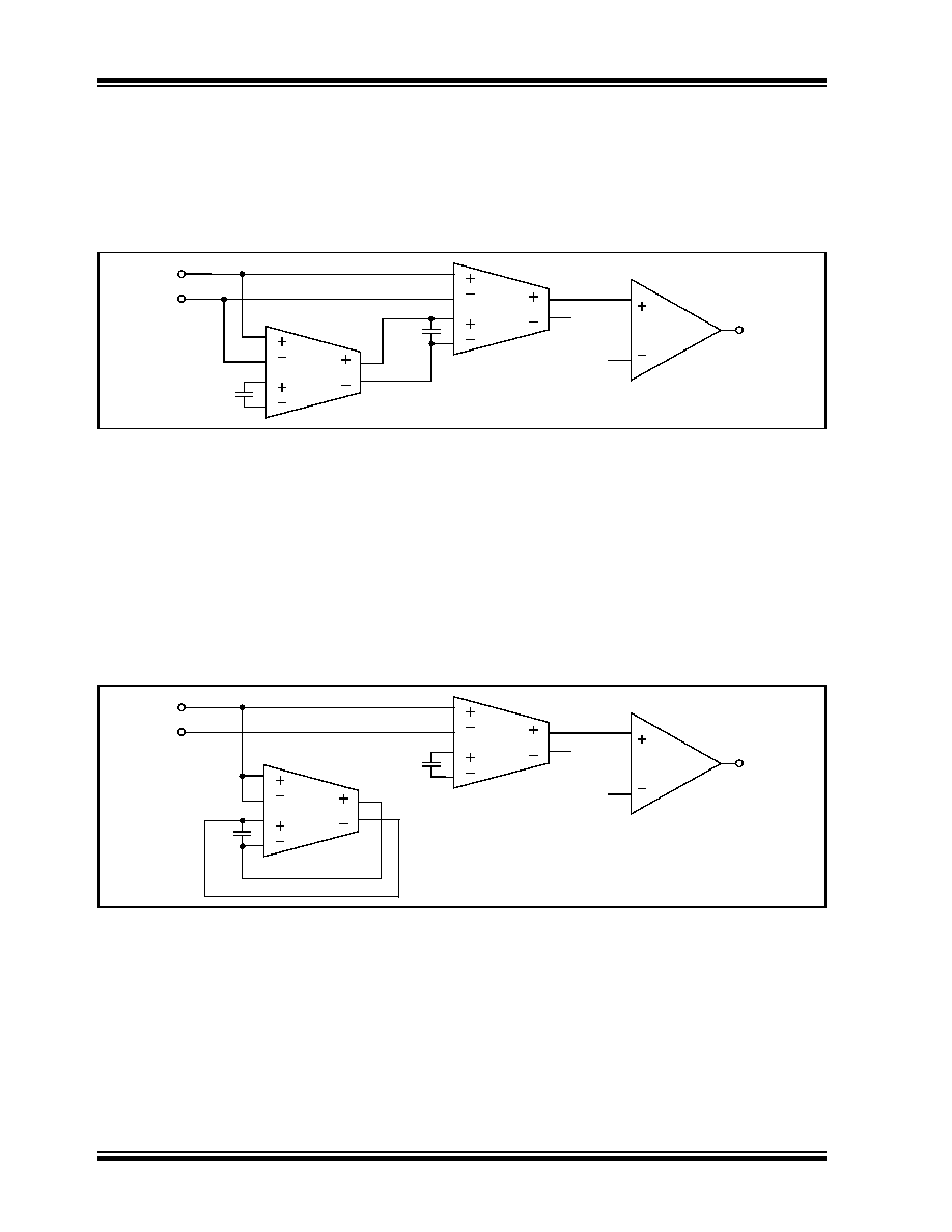
4.1.2
AUTO-ZEROING ACTION
Figure 4-2 shows the connections between amplifiers
during the Normal Mode of operation (
φ1). The hold
capacitor (CH) corrects the Null Amplifier’s input offset.
Since the Null Amplifier has very high gain, it
dominates the signal seen by the Main Amplifier. This
greatly reduces the impact of the Main Amplifier’s input
offset voltage on overall performance. Essentially, the
Null Amplifier and Main Amplifier behave as a regular
op amp with very high gain (AOL) and very low offset
voltage (VOS).
FIGURE 4-2:
Normal Mode of Operation (
φ
1); Equivalent Amplifier Diagram.
Figure 4-3 shows the connections between amplifiers
during the Auto-zeroing Mode of operation (
φ2). The
signal goes directly through the Main Amplifier, and the
flywheel capacitor (CFW) maintains a constant correc-
tion on the Main Amplifier’s offset.
The Null Amplifier uses its own high open loop gain to
drive the voltage across CH to the point where its input
offset voltage is almost zero. Because the signal input
pair is connected to VIN+, the auto-zeroing action
corrects the offset at the current common mode input
voltage (VCM) and supply voltage (VDD). This makes
the DC CMRR and PSRR very high also.
Since these corrections happen every 40 s, or so, we
also minimize slow errors, including offset drift with
temperature (
ΔVOS/ΔTA), 1/f noise, and input offset
aging.
FIGURE 4-3:
Auto-zeroing Mode of Operation (
φ
2); Equivalent Diagram.
4.1.3
INTERMODULATION DISTORTION
(IMD)
The MCP6V26/7/8 op amps will show intermodulation
distortion (IMD), products when an AC signal is
present.
The signal and clock can be decomposed into sine
wave tones (Fourier series components). These tones
interact with the auto-zeroing circuitry’s non-linear
response to produce IMD tones at sum and difference
frequencies. Each of the square wave clock’s
harmonics has a series of IMD tones centered on it.
See Figure 2-37 and Figure 2-38.
VIN+
VIN–
Main
Output
VOUT
VREF
Amp.
Buffer
NC
Null
Amp.
CH
CFW
VIN+
VIN–
Main
Output
VOUT
VREF
Amp.
Buffer
NC
Null
Amp.
CH
CFW
相关PDF资料 |
PDF描述 |
|---|---|
| BZW04-213-E3/54 | TVS 400W 213V 5% UNIDIR DO-204AL |
| TSW-120-14-S-D | CONN HEADER 40POS .100" DL GOLD |
| SSQ-103-03-T-S-RA | CONN RCPT .100" 3PS R/A SGL TIN |
| 1.5KE33A-E3/54 | TVS UNIDIR 1.5KW 33V 5% 1.5KE |
| PBC19DGBN | CONN HEADER .100 DUAL R/A 38POS |
相关代理商/技术参数 |
参数描述 |
|---|---|
| MCP6V27T-E/MD | 功能描述:运算放大器 - 运放 620 uA, 2 MHz Auto-Zeroed Op Amps RoHS:否 制造商:STMicroelectronics 通道数量:4 共模抑制比(最小值):63 dB 输入补偿电压:1 mV 输入偏流(最大值):10 pA 工作电源电压:2.7 V to 5.5 V 安装风格:SMD/SMT 封装 / 箱体:QFN-16 转换速度:0.89 V/us 关闭:No 输出电流:55 mA 最大工作温度:+ 125 C 封装:Reel |
| MCP6V27T-E/MS | 功能描述:运算放大器 - 运放 620 uA, 2 MHz Auto-Zeroed Op Amps RoHS:否 制造商:STMicroelectronics 通道数量:4 共模抑制比(最小值):63 dB 输入补偿电压:1 mV 输入偏流(最大值):10 pA 工作电源电压:2.7 V to 5.5 V 安装风格:SMD/SMT 封装 / 箱体:QFN-16 转换速度:0.89 V/us 关闭:No 输出电流:55 mA 最大工作温度:+ 125 C 封装:Reel |
| MCP6V27T-E/SN | 功能描述:运算放大器 - 运放 620 uA, 2 MHz Auto-Zeroed Op Amps RoHS:否 制造商:STMicroelectronics 通道数量:4 共模抑制比(最小值):63 dB 输入补偿电压:1 mV 输入偏流(最大值):10 pA 工作电源电压:2.7 V to 5.5 V 安装风格:SMD/SMT 封装 / 箱体:QFN-16 转换速度:0.89 V/us 关闭:No 输出电流:55 mA 最大工作温度:+ 125 C 封装:Reel |
| MCP6V28-E/MS | 功能描述:运算放大器 - 运放 Sngl, Auto-0 Op Amp w/ Chip Select,E Tmp RoHS:否 制造商:STMicroelectronics 通道数量:4 共模抑制比(最小值):63 dB 输入补偿电压:1 mV 输入偏流(最大值):10 pA 工作电源电压:2.7 V to 5.5 V 安装风格:SMD/SMT 封装 / 箱体:QFN-16 转换速度:0.89 V/us 关闭:No 输出电流:55 mA 最大工作温度:+ 125 C 封装:Reel |
| MCP6V28-E/SN | 功能描述:运算放大器 - 运放 Sngl, Auto-0 Op Amp w/ Chip Select,E Tmp RoHS:否 制造商:STMicroelectronics 通道数量:4 共模抑制比(最小值):63 dB 输入补偿电压:1 mV 输入偏流(最大值):10 pA 工作电源电压:2.7 V to 5.5 V 安装风格:SMD/SMT 封装 / 箱体:QFN-16 转换速度:0.89 V/us 关闭:No 输出电流:55 mA 最大工作温度:+ 125 C 封装:Reel |
发布紧急采购,3分钟左右您将得到回复。