参数资料
| 型号: | MCP6V27-E/MS |
| 厂商: | Microchip Technology |
| 文件页数: | 16/50页 |
| 文件大小: | 0K |
| 描述: | IC OPAMP DUAL AUTO-ZERO 8MSOP |
| 标准包装: | 100 |
| 放大器类型: | 自动调零 |
| 电路数: | 2 |
| 输出类型: | 满摆幅 |
| 转换速率: | 1 V/µs |
| 增益带宽积: | 2MHz |
| 电流 - 输入偏压: | 7pA |
| 电压 - 输入偏移: | 2µV |
| 电流 - 电源: | 620µA |
| 电流 - 输出 / 通道: | 22mA |
| 电压 - 电源,单路/双路(±): | 2.3 V ~ 5.5 V |
| 工作温度: | -40°C ~ 125°C |
| 安装类型: | 表面贴装 |
| 封装/外壳: | 8-TSSOP,8-MSOP(0.118",3.00mm 宽) |
| 供应商设备封装: | 8-MSOP |
| 包装: | 管件 |
第1页第2页第3页第4页第5页第6页第7页第8页第9页第10页第11页第12页第13页第14页第15页当前第16页第17页第18页第19页第20页第21页第22页第23页第24页第25页第26页第27页第28页第29页第30页第31页第32页第33页第34页第35页第36页第37页第38页第39页第40页第41页第42页第43页第44页第45页第46页第47页第48页第49页第50页
2011 Microchip Technology Inc.
DS25007B-page 23
MCP6V26/7/8
4.2
Other Functional Blocks
4.2.1
RAIL-TO-RAIL INPUTS
The input stage of the MCP6V26/7/8 op amps use two
differential CMOS input stages in parallel. One
operates at low common mode input voltage (VCM,
which is approximately equal to VIN+ and VIN– in
normal operation) and the other at high VCM. With this
topology, the input operates with VCM up to VDD +0.2V,
The input offset voltage (VOS) is measured at
VCM =VSS – 0.15V and VDD + 0.2V to ensure proper
operation.
The transition between the input stages occurs when
the best distortion and gain linearity, with non-inverting
gains, avoid this region of operation.
4.2.1.1
Phase Reversal
The input devices are designed to not exhibit phase
inversion when the input pins exceed the supply
voltages.
Figure 2-43 shows
an
input voltage
exceeding both supplies with no phase inversion.
4.2.1.2
Input Voltage Limits
In order to prevent damage and/or improper operation
of these amplifiers, the circuit must limit the voltages at
the input pins (see Section 1.1, Absolute Maximum
Ratings ). This requirement is independent of the
current limits discussed later on.
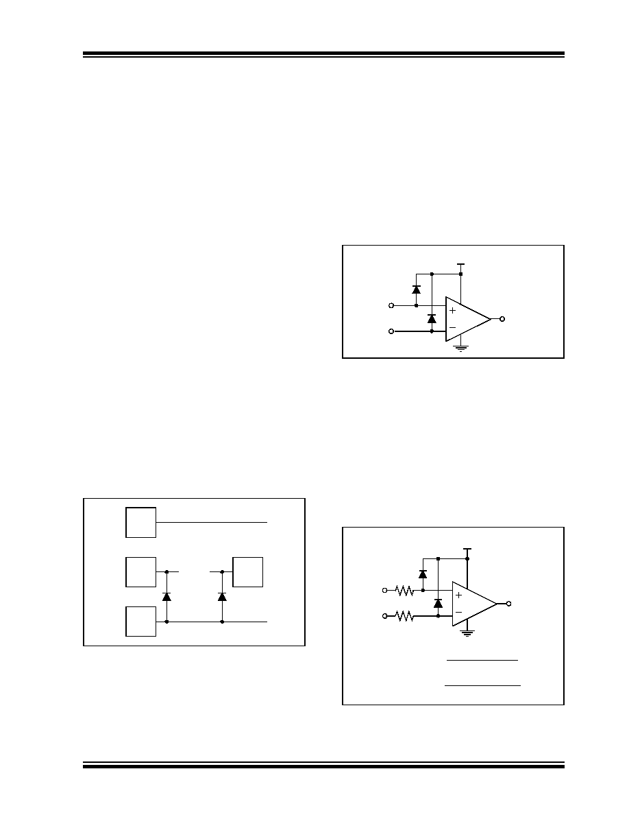
The ESD protection on the inputs can be depicted as
shown in Figure 4-4. This structure was chosen to
protect the input transistors against many (but not all)
over-voltage conditions, and to minimize input bias
current (IB).
FIGURE 4-4:
Simplified Analog Input ESD
Structures.
The input ESD diodes clamp the inputs when they try
to go more than one diode drop below VSS. They also
clamp any voltages that are well above VDD; their
breakdown voltage is high enough to allow normal
operation, but not low enough to protect against slow
over-voltage (beyond VDD) events. Very fast ESD
events (that meet the spec) are limited so that damage
does not occur.
In some applications, it may be necessary to prevent
excessive voltages from reaching the op amp inputs;
Figure 4-5 shows one approach to protecting these
inputs. D1 and D2 may be small signal silicon diodes,
Schottky diodes for lower clamping voltages or diode-
connected FETs for low leakage.
FIGURE 4-5:
Protecting the Analog Inputs
Against High Voltages.
4.2.1.3
Input Current Limits
In order to prevent damage and/or improper operation
of these amplifiers, the circuit must limit the currents
into the input pins (see Section 1.1, Absolute
This
requirement
is
independent of the voltage limits previously discussed.
Figure 4-6 shows one approach to protecting these
inputs. The resistors R1 and R2 limit the possible
current in or out of the input pins (and into D1 and D2).
The diode currents will dump onto VDD.
FIGURE 4-6:
Protecting the Analog Inputs
Against High Currents.
Bond
Pad
Bond
Pad
Bond
Pad
VDD
VIN+
VSS
Input
Stage
Bond
Pad
VIN–
V1
VDD
D1
VOUT
V2
D2
U1
MCP6V2X
V1
R1
VDD
D1
min(R1,R2)>
VSS –min(V1,V2)
2mA
VOUT
V2
R2
D2
min(R1,R2)>
max(V1,V2)– VDD
2mA
U1
MCP6V2X
相关PDF资料 |
PDF描述 |
|---|---|
| SMCJ7.0CA-13-F | TVS BIDIRECT 1500W 7.0V SMC |
| TLC2274CD | IC OPAMP GP R-R 2.25MHZ 14SOIC |
| SMCJ75CA-13-F | TVS BIDIRECT 1500W 75V SMC |
| SMCJ24CA-13-F | TVS BIDIRECT 1500W 24V SMC |
| SMCJ33CA-13-F | TVS BIDIRECT 1500W 33V SMC |
相关代理商/技术参数 |
参数描述 |
|---|---|
| MCP6V27T-E/MD | 功能描述:运算放大器 - 运放 620 uA, 2 MHz Auto-Zeroed Op Amps RoHS:否 制造商:STMicroelectronics 通道数量:4 共模抑制比(最小值):63 dB 输入补偿电压:1 mV 输入偏流(最大值):10 pA 工作电源电压:2.7 V to 5.5 V 安装风格:SMD/SMT 封装 / 箱体:QFN-16 转换速度:0.89 V/us 关闭:No 输出电流:55 mA 最大工作温度:+ 125 C 封装:Reel |
| MCP6V27T-E/MS | 功能描述:运算放大器 - 运放 620 uA, 2 MHz Auto-Zeroed Op Amps RoHS:否 制造商:STMicroelectronics 通道数量:4 共模抑制比(最小值):63 dB 输入补偿电压:1 mV 输入偏流(最大值):10 pA 工作电源电压:2.7 V to 5.5 V 安装风格:SMD/SMT 封装 / 箱体:QFN-16 转换速度:0.89 V/us 关闭:No 输出电流:55 mA 最大工作温度:+ 125 C 封装:Reel |
| MCP6V27T-E/SN | 功能描述:运算放大器 - 运放 620 uA, 2 MHz Auto-Zeroed Op Amps RoHS:否 制造商:STMicroelectronics 通道数量:4 共模抑制比(最小值):63 dB 输入补偿电压:1 mV 输入偏流(最大值):10 pA 工作电源电压:2.7 V to 5.5 V 安装风格:SMD/SMT 封装 / 箱体:QFN-16 转换速度:0.89 V/us 关闭:No 输出电流:55 mA 最大工作温度:+ 125 C 封装:Reel |
| MCP6V28-E/MS | 功能描述:运算放大器 - 运放 Sngl, Auto-0 Op Amp w/ Chip Select,E Tmp RoHS:否 制造商:STMicroelectronics 通道数量:4 共模抑制比(最小值):63 dB 输入补偿电压:1 mV 输入偏流(最大值):10 pA 工作电源电压:2.7 V to 5.5 V 安装风格:SMD/SMT 封装 / 箱体:QFN-16 转换速度:0.89 V/us 关闭:No 输出电流:55 mA 最大工作温度:+ 125 C 封装:Reel |
| MCP6V28-E/SN | 功能描述:运算放大器 - 运放 Sngl, Auto-0 Op Amp w/ Chip Select,E Tmp RoHS:否 制造商:STMicroelectronics 通道数量:4 共模抑制比(最小值):63 dB 输入补偿电压:1 mV 输入偏流(最大值):10 pA 工作电源电压:2.7 V to 5.5 V 安装风格:SMD/SMT 封装 / 箱体:QFN-16 转换速度:0.89 V/us 关闭:No 输出电流:55 mA 最大工作温度:+ 125 C 封装:Reel |
发布紧急采购,3分钟左右您将得到回复。