- 您现在的位置:买卖IC网 > PDF目录9389 > MCP79512T-I/MN (Microchip Technology)IC RTCC SPI 64B SRAM 10-TDFN PDF资料下载
参数资料
| 型号: | MCP79512T-I/MN |
| 厂商: | Microchip Technology |
| 文件页数: | 14/17页 |
| 文件大小: | 0K |
| 描述: | IC RTCC SPI 64B SRAM 10-TDFN |
| 标准包装: | 3,300 |
| 类型: | 时钟/日历 |
| 特点: | 警报器,EEPROM,闰年,方波输出,SRAM,唯一 ID |
| 存储容量: | 64B |
| 时间格式: | HH:MM:SS:hh(12/24 小时) |
| 数据格式: | YY-MM-DD-dd |
| 接口: | SPI |
| 电源电压: | 1.8 V ~ 3.6 V |
| 电压 - 电源,电池: | 1.3 V ~ 3.6 V |
| 工作温度: | -40°C ~ 85°C |
| 安装类型: | 表面贴装 |
| 封装/外壳: | 10-WFDFN 裸露焊盘 |
| 供应商设备封装: | 10-TDFN(3x3) |
| 包装: | 带卷 (TR) |
MCP7952X/MCP7951X
DS22300A-page 6
Preliminary
2012 Microchip Technology Inc.
2.0
PIN DESCRIPTION
The descriptions of the pins are listed in Table 2-1.
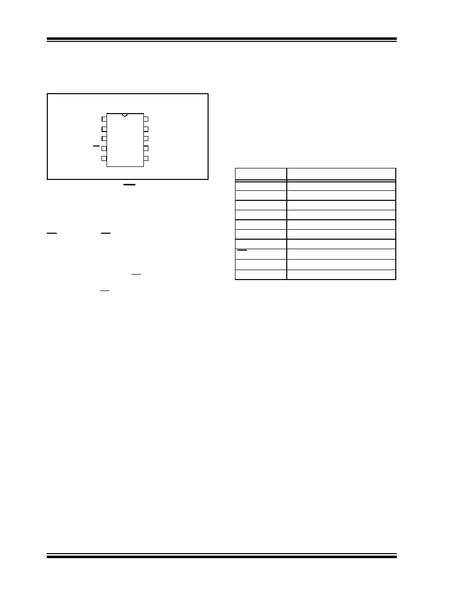
FIGURE 2-1:
DEVICE PINOUTS
2.1
Chip Select (CS)
A low level on this pin selects the device. A high level
deselects the device and forces it into Standby mode.
However, a programming cycle which is already initi-
ated or in progress will be completed, regardless of the
CS input signal. If CS is brought high during a program
cycle, the device will go in Standby mode as soon as
the programming cycle is complete. When the device is
deselected, SO goes into the high-impedance state,
allowing multiple parts to share the same SPI bus. A
low-to-high transition on CS after a valid write
sequence initiates an internal write cycle. After power-
up, a low level on CS is required prior to any sequence
being initiated.
2.2
Serial Output (SO)
The SO pin is used to transfer data out of the
MCP795XX. During a read cycle, data is shifted out on
this pin after the falling edge of the serial clock.
2.3
Serial Input (SI)
The SI pin is used to transfer data into the device. It
receives instructions, addresses and data. Data is
latched on the rising edge of the serial clock.
2.4
Serial Clock (SCK)
The SCK is used to synchronize the communication
between a master and the MCP795XX. Instructions,
addresses or data present on the SI pin are latched on
the rising edge of the clock input, while data on the SO
pin is updated after the falling edge of the clock input.
2.5
Multifunction Pin (MFP)
The MFP pin is shared with the clock divider and the
alarms. This pin requires an external pull-up to VCC or
VBAT. The pin remains low until such time that the inter-
rupt flag in the register is cleared by software. This pin
has a maximum sink current of 10mA.
2.6
X1, X2
The X1 and X2 pins connect to the on-board oscillator
block. X1 is the input to the module and X2 is the out-
put of the module. The device can be run from an
external CMOS signal by feeding into the X1 pin. If
driving X1 the X2 pin should be a No Connect.
2.7
VBAT
The VBAT pin is a secondary supply input to maintain
the Clock and SRAM contents when VCC is removed.
TABLE 2-1:
PIN DESCRIPTIONS
X1
X2
VBAT
Vcc
MFP
1
2
3
4
MC
P
795X
X
MSOP/TDFN
CS
VSS
SCK
SO
SI
5
6
7
10
9
8
Pin Name
Pin Function
VSS
Ground
X1
Xtal Input, External Oscillator Input
X2
Xtal Output
VBAT
Battery Backup Input (3V Typ)
VCC
+1.8V to +3.6V Power Supply
SI
Serial Input
SCK
Serial Clock
CS
Chip Select
MFP
Multifunction Pin
SO
Serial Output
相关PDF资料 |
PDF描述 |
|---|---|
| M83723/86R2016N | CONN PLUG 16POS STRAIGHT W/SCKT |
| MCP4231-502E/SL | IC DGTL POT DUAL 5K 2CH 14SOIC |
| VI-B3Z-MW-F4 | CONVERTER MOD DC/DC 2V 40W |
| VI-B3P-MW-B1 | CONVERTER MOD DC/DC 13.8V 100W |
| MCP79511T-I/MS | IC RTCC SPI 64B SRAM 10-MSOP |
相关代理商/技术参数 |
参数描述 |
|---|---|
| MCP7951X | 制造商:MAS 制造商全称:MAS 功能描述:3V SPI Real-Time Clock Calendar with Battery Switchover |
| MCP79520 | 制造商:MAS 制造商全称:MAS 功能描述:3V SPI Real-Time Clock Calendar with Battery Switchover |
| MCP79520-I/MS | 功能描述:实时时钟 SPI GP RTCC 2Kb EE 64B SRAM ID RoHS:否 制造商:Microchip Technology 功能:Clock, Calendar. Alarm RTC 总线接口:I2C 日期格式:DW:DM:M:Y 时间格式:HH:MM:SS RTC 存储容量:64 B 电源电压-最大:5.5 V 电源电压-最小:1.8 V 最大工作温度:+ 85 C 最小工作温度: 安装风格:Through Hole 封装 / 箱体:PDIP-8 封装:Tube |
| MCP79520T-I/MN | 功能描述:实时时钟 SPI GP RTCC 2Kb EE 64B SRAM ID RoHS:否 制造商:Microchip Technology 功能:Clock, Calendar. Alarm RTC 总线接口:I2C 日期格式:DW:DM:M:Y 时间格式:HH:MM:SS RTC 存储容量:64 B 电源电压-最大:5.5 V 电源电压-最小:1.8 V 最大工作温度:+ 85 C 最小工作温度: 安装风格:Through Hole 封装 / 箱体:PDIP-8 封装:Tube |
| MCP79520T-I/MS | 功能描述:实时时钟 SPI GP RTCC 2Kb EE 64B SRAM ID RoHS:否 制造商:Microchip Technology 功能:Clock, Calendar. Alarm RTC 总线接口:I2C 日期格式:DW:DM:M:Y 时间格式:HH:MM:SS RTC 存储容量:64 B 电源电压-最大:5.5 V 电源电压-最小:1.8 V 最大工作温度:+ 85 C 最小工作温度: 安装风格:Through Hole 封装 / 箱体:PDIP-8 封装:Tube |
发布紧急采购,3分钟左右您将得到回复。