- 您现在的位置:买卖IC网 > PDF目录9388 > MCP795W20T-I/SL (Microchip Technology)IC RTCC 2KB EE WD/EVENT 14SOIC PDF资料下载
参数资料
| 型号: | MCP795W20T-I/SL |
| 厂商: | Microchip Technology |
| 文件页数: | 4/13页 |
| 文件大小: | 0K |
| 描述: | IC RTCC 2KB EE WD/EVENT 14SOIC |
| 标准包装: | 2,600 |
| 类型: | 时钟/日历 |
| 特点: | 警报,EEPROM,闰年,方波输出,SRAM,看门狗定时器 |
| 存储容量: | 64B |
| 时间格式: | HH:MM:SS:hh(12/24 小时) |
| 数据格式: | YY-MM-DD-dd |
| 接口: | SPI |
| 电源电压: | 1.8 V ~ 5.5 V |
| 电压 - 电源,电池: | 1.3 V ~ 5.5 V |
| 工作温度: | -40°C ~ 85°C |
| 安装类型: | 表面贴装 |
| 封装/外壳: | 14-SOIC(0.154",3.90mm 宽) |
| 供应商设备封装: | 14-SOIC |
| 包装: | 带卷 (TR) |
2010 Microchip Technology Inc.
DS22250A-page 27
MCP4902/4912/4922
6.0
TYPICAL APPLICATIONS
The MCP4902/4912/4922 family of devices are gen-
eral purpose DACs intended to be used in applications
where a precision with low-power and moderate
bandwidth is required.
Applications generally suited for the devices are:
Set Point or Offset Trimming
Sensor Calibration
Digitally-Controlled Multiplier/Divider
Portable Instrumentation (Battery Powered)
Motor Control Feedback Loop
6.1
Digital Interface
The MCP4902/4912/4922 utilizes a 3-wire synchro-
nous serial protocol to transfer the DAC’s setup and
output values from the digital source. The serial proto-
col can be interfaced to SPI or Microwire peripherals
that is common on many microcontroller units (MCUs),
including Microchip’s PIC MCUs and dsPIC DSCs.
In addition to the three serial connections (CS, SCK
and SDI), the LDAC signal synchronizes the two DAC
outputs. By bringing down the LDAC pin to “low”, all
DAC input codes and settings in the two DAC input
registers are latched into their DAC output registers at
the same time. Therefore, both DACA and DACB
outputs are updated at the same time. Figure 6-1
shows an example of the pin connections. Note that the
LDAC pin can be tied low (VSS) to reduce the required
connections from 4 to 3 I/O pins. In this case, the DAC
output can be immediately updated when a valid
16-clock transmission has been received and CS pin
has been raised.
6.2
Power Supply Considerations
The typical application will require a bypass capacitor
in order to filter high-frequency noise. The noise can be
induced onto the power supply’s traces from various
events such as digital switching or as a result of
changes on the DAC’s output. The bypass capacitor
helps to minimize the effect of these noise sources.
Figure 6-1 illustrates an appropriate bypass strategy. In
this example, two bypass capacitors are used in
parallel: (a) 0.1 F (ceramic) and (b) 10 F (tantalum).
These capacitors should be placed as close to the
device power pin (VDD) as possible (within 4 mm).
The power source supplying these devices should be
as clean as possible. If the application circuit has
separate digital and analog power supplies, VDD and
VSS should reside on the analog plane.
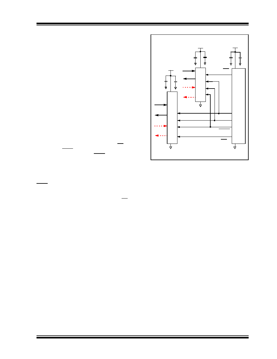
FIGURE 6-1:
Typical Connection
Diagram.
6.3
Layout Considerations
Inductively-coupled AC transients and digital switching
noises can degrade the input and output signal
integrity, and potentially reduce the device perfor-
mance. Careful board layout will minimize these effects
and increase the Signal-to-Noise Ratio (SNR). Bench
testing has shown that a multi-layer board utilizing a
low-inductance ground plane, isolated inputs and
isolated outputs with proper decoupling, is critical for
the best performance. Particularly harsh environments
may require shielding of critical signals.
Breadboards and wire-wrapped boards are not
recommended if low noise is desired.
VDD
AVSS
VSS
VREFA
VOUTA
VREFB
VOUTB
PIC
M
icroc
ontrol
ler
VREFA
VOUTA
VREFB
VOUTB
SDI
CS1
SDO
SCK
LDAC
CS0
C1
C2
MC
P4
9x2
MC
P
4
9x
2
C1
C1 = 10 F
C2 = 0.1 F
相关PDF资料 |
PDF描述 |
|---|---|
| MCP795W12T-I/SL | IC RTCC 1KB EE WD/EVENT 14SOIC |
| VE-J0L-MZ | CONVERTER MOD DC/DC 28V 25W |
| MS27484T24A35P | CONN PLUG 128POS STRAIGHT W/PINS |
| VE-J0K-MZ | CONVERTER MOD DC/DC 40V 25W |
| MS27473E16B6PD | CONN PLUG 6POS STRAIGHT W/PINS |
相关代理商/技术参数 |
参数描述 |
|---|---|
| MCP795W21 | 制造商:MAS 制造商全称:MAS 功能描述:SPI Real-Time Clock Calendar |
| MCP795W21-I/SL | 功能描述:实时时钟 2Kb EE 64B SRAM WD TED EUI-48 RoHS:否 制造商:Microchip Technology 功能:Clock, Calendar. Alarm RTC 总线接口:I2C 日期格式:DW:DM:M:Y 时间格式:HH:MM:SS RTC 存储容量:64 B 电源电压-最大:5.5 V 电源电压-最小:1.8 V 最大工作温度:+ 85 C 最小工作温度: 安装风格:Through Hole 封装 / 箱体:PDIP-8 封装:Tube |
| MCP795W21-I/ST | 功能描述:实时时钟 2Kb EE 64B SRAM WD TED EUI-48 RoHS:否 制造商:Microchip Technology 功能:Clock, Calendar. Alarm RTC 总线接口:I2C 日期格式:DW:DM:M:Y 时间格式:HH:MM:SS RTC 存储容量:64 B 电源电压-最大:5.5 V 电源电压-最小:1.8 V 最大工作温度:+ 85 C 最小工作温度: 安装风格:Through Hole 封装 / 箱体:PDIP-8 封装:Tube |
| MCP795W21T-I/SL | 功能描述:实时时钟 2Kb EE 64B SRAM WD TED EUI-48 RoHS:否 制造商:Microchip Technology 功能:Clock, Calendar. Alarm RTC 总线接口:I2C 日期格式:DW:DM:M:Y 时间格式:HH:MM:SS RTC 存储容量:64 B 电源电压-最大:5.5 V 电源电压-最小:1.8 V 最大工作温度:+ 85 C 最小工作温度: 安装风格:Through Hole 封装 / 箱体:PDIP-8 封装:Tube |
| MCP795W21T-I/ST | 功能描述:实时时钟 2Kb EE 64B SRAM WD TED EUI-48 RoHS:否 制造商:Microchip Technology 功能:Clock, Calendar. Alarm RTC 总线接口:I2C 日期格式:DW:DM:M:Y 时间格式:HH:MM:SS RTC 存储容量:64 B 电源电压-最大:5.5 V 电源电压-最小:1.8 V 最大工作温度:+ 85 C 最小工作温度: 安装风格:Through Hole 封装 / 箱体:PDIP-8 封装:Tube |
发布紧急采购,3分钟左右您将得到回复。