- 您现在的位置:买卖IC网 > PDF目录9429 > MCP795W22-I/ST (Microchip Technology)IC RTCC 64B SRAM WD/DET 14TSSOP PDF资料下载
参数资料
| 型号: | MCP795W22-I/ST |
| 厂商: | Microchip Technology |
| 文件页数: | 13/13页 |
| 文件大小: | 0K |
| 描述: | IC RTCC 64B SRAM WD/DET 14TSSOP |
| 标准包装: | 96 |
| 类型: | 时钟/日历 |
| 特点: | 警报,EEPROM,闰年,方波输出,SRAM,唯一 ID,看门狗定时器 |
| 存储容量: | 64B |
| 时间格式: | HH:MM:SS:hh(12/24 小时) |
| 数据格式: | YY-MM-DD-dd |
| 接口: | SPI |
| 电源电压: | 1.8 V ~ 5.5 V |
| 电压 - 电源,电池: | 1.3 V ~ 5.5 V |
| 工作温度: | -40°C ~ 85°C |
| 安装类型: | 表面贴装 |
| 封装/外壳: | 14-TSSOP(0.173",4.40mm 宽) |
| 供应商设备封装: | 14-TSSOP |
| 包装: | 管件 |
MCP795W1X/MCP795W2X
DS22280C-page 8
Preliminary
2011-2012 Microchip Technology Inc.
3.0
SPI BUS OPERATION
The MCP795WXX is designed to interface directly with
the Serial Peripheral Interface (SPI) port of many of
today’s popular microcontroller families, including
Microchip’s PIC microcontrollers. It may also interface
with microcontrollers that do not have a built-in SPI port
by using discrete I/O lines programmed properly in
software to match the SPI protocol.
The MCP795WXX contains an 8-bit instruction register.
The device is accessed via the SI pin, with data being
clocked in on the rising edge of SCK. The CS pin must
be low for the entire operation.
Table 3-1 contains a list of the possible instruction
bytes and format for device operation. All instructions,
addresses, and data are transferred MSb first, LSb last.
Data (SI) is sampled on the first rising edge of SCK
after CS goes low.
TABLE 3-1:
INSTRUCTION SET SUMMARY
3.1
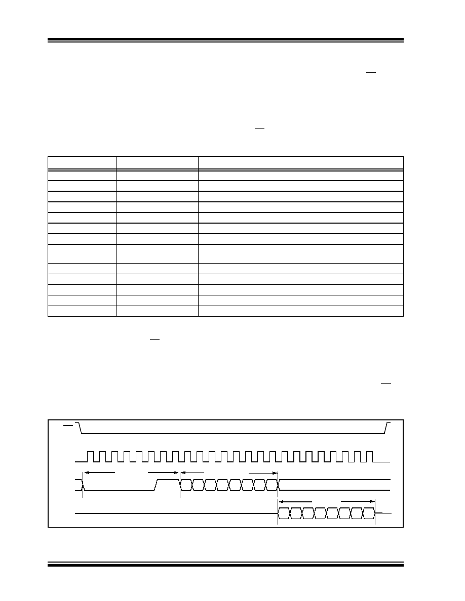
Read Sequence
The device is selected by pulling CS low. The various
8-bit read instructions are transmitted to the
MCP795WXX followed by an 8-bit address. See
Figure 3-1 for more details.
After the correct instruction and address are sent, the
data stored in the memory at the selected address is
shifted out on the SO pin. Data stored in the memory at
the next address can be read sequentially by
continuing to provide clock pulses to the slave. The
internal Address Pointer automatically increments to
the next higher address after each byte of data is
shifted out. When the highest address is reached, the
address counter rolls over to the first valid address
allowing the read cycle to be continued indefinitely. The
read operation is terminated by raising the CS pin
(Figure 1-1).
FIGURE 3-1:
EEREAD SEQUENCE
Instruction Name
Instruction Format
Description
EEREAD
0000 0011
Read data from EE memory array beginning at selected address
EEWRITE
0000 0010
Write data to EE memory array beginning at selected address
EEWRDI
0000 0100
Reset the write enable latch (disable write operations)
EEWREN
0000 0110
Set the write enable latch (enable write operations)
SRREAD
0000 0101
Read STATUS register
SRWRITE
0000 0001
Write STATUS register
READ
0001 0011
Read RTCC/SRAM array beginning at selected address
WRITE
0001 0010
Write RTCC/SRAM data to memory array beginning at selected
address
UNLOCK
0001 0100
Unlock ID Locations
IDWRITE
0011 0010
Write to the ID Locations
IDREAD
0011 0011
Read the ID Locations
CLRWDT
0100 0100
Clear Watchdog TImer
CLRRAM
0101 0100
Clear RAM Location to ‘0’
SO
SI
SCK
CS
0
23456
789 10 11
1
01
0
01
A7 A6 A5 A4
A1 A0
76543210
Data Out
High-Impedance
A3 A2
Address Byte
12 13 14 15 16 17 18 19 20 21 22 23
Instruction
相关PDF资料 |
PDF描述 |
|---|---|
| VE-B2L-MX-B1 | CONVERTER MOD DC/DC 28V 75W |
| VE-B2K-MX-B1 | CONVERTER MOD DC/DC 40V 75W |
| AD5263BRUZ20-REEL7 | IC DGTL POT QUAD 20K 24-TSSOP |
| MS3450W12S-4P | CONN RCPT 1POS WALL MNT W/PINS |
| VE-B22-MX-B1 | CONVERTER MOD DC/DC 15V 75W |
相关代理商/技术参数 |
参数描述 |
|---|---|
| MCP795W22T-I/SL | 功能描述:实时时钟 2Kb EE 64B SRAM WD TED EUI-64 RoHS:否 制造商:Microchip Technology 功能:Clock, Calendar. Alarm RTC 总线接口:I2C 日期格式:DW:DM:M:Y 时间格式:HH:MM:SS RTC 存储容量:64 B 电源电压-最大:5.5 V 电源电压-最小:1.8 V 最大工作温度:+ 85 C 最小工作温度: 安装风格:Through Hole 封装 / 箱体:PDIP-8 封装:Tube |
| MCP795W22T-I/ST | 功能描述:实时时钟 2Kb EE 64B SRAM WD TED EUI-64 RoHS:否 制造商:Microchip Technology 功能:Clock, Calendar. Alarm RTC 总线接口:I2C 日期格式:DW:DM:M:Y 时间格式:HH:MM:SS RTC 存储容量:64 B 电源电压-最大:5.5 V 电源电压-最小:1.8 V 最大工作温度:+ 85 C 最小工作温度: 安装风格:Through Hole 封装 / 箱体:PDIP-8 封装:Tube |
| MCP795W2X | 制造商:MICROCHIP 制造商全称:Microchip Technology 功能描述:3V SPI Real-Time Clock Calendar with Enhanced Features and Battery Switchover |
| MCP795WXX | 制造商:MAS 制造商全称:MAS 功能描述:SPI Real-Time Clock Calendar |
| MCP7M | 制造商:Preh Elec. 功能描述: |
发布紧急采购,3分钟左右您将得到回复。