- 您现在的位置:买卖IC网 > PDF目录20365 > MCZ33198EFR2 (Freescale Semiconductor)IC TMOS DRIVER AUTO HISIDE 8SOIC PDF资料下载
参数资料
| 型号: | MCZ33198EFR2 |
| 厂商: | Freescale Semiconductor |
| 文件页数: | 13/17页 |
| 文件大小: | 0K |
| 描述: | IC TMOS DRIVER AUTO HISIDE 8SOIC |
| 标准包装: | 2,500 |
| 配置: | 高端 |
| 输入类型: | 非反相 |
| 延迟时间: | 1ms |
| 配置数: | 1 |
| 输出数: | 1 |
| 电源电压: | 7 V ~ 20 V |
| 工作温度: | -40°C ~ 125°C |
| 安装类型: | 表面贴装 |
| 封装/外壳: | 8-SOIC(0.154",3.90mm 宽) |
| 供应商设备封装: | 8-SOICN |
| 包装: | 带卷 (TR) |
�� �
�
�FUNCTIONAL� DESCRIPTION�
�INTRODUCTION�
�the� switch� off� time� can� be� long,� compared� to� the� on-switching�
�time� response.� This� is� due� to� the� 110mA� gate� discharge�
�current.� To� improve� this� parameter,� a� resistor� can� be� added�
�Table� 6.� Switching� Off� Characteristics� with� MOSFET�
�Additional� Gate� Resistor�
�in� parallel� with� the� gate� of� the� MOSFET.� See� Figures 16� and�
�17� .�
�Vbat�
�Vbat�
�R� GATE� (R� G� )�
�No� R�
�VCC� (V)�
�7.0�
�10�
�14�
�20�
�7.0�
�V� GATE� (V)�
�16�
�23�
�28�
�34�
�14�
�T� OFF� (� μ� s� ec)�
�450�
�700�
�750�
�780�
�160�
�4�
�1�
�1K�
�68� k� ?�
�10�
�14�
�22�
�27�
�230�
�230�
�20�
�33�
�220�
�3�
�Rg�
�LOAD�
�39� k� ?�
�7.0�
�10�
�13�
�21�
�100�
�160�
�Figure� 16.� Schematic� with� R� GATE� Resistor�
�14�
�20�
�7.0�
�26�
�32�
�11�
�160�
�150�
�30�
�5V�
�INPUT� SIGNAL� PIN7�
�0V�
�15� k� ?�
�10�
�14�
�20�
�17.5�
�24�
�28.5�
�50�
�50�
�50�
�Vcc� +� 15V� typ�
�Vgate� WITHOUT� Rgate�
�Notes�
�1.� Time� from� negative� edge� of� input� signal� (Pin� 7)� to� negative�
�edge� of� gate� voltage� (Pin� 4)� measured� at� 5V� threshold.�
�2.� Gate� discharge� time,� not� LOAD� switching� OFF� time.L�
�0V�
�Vgate� WITH� Rgate�
�3.� TMOS� used� is� Freescale� MTP50N06,� load� 10� ?� resistor.�
�Toff�
�Figure� 17.� R� GATE� Signal� Comparison�
�Toff�
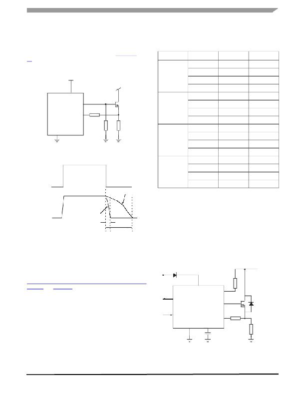
�REVERSE� BATTERY�
�The� device� does� not� sustain� reverse� battery� operation� for�
�V� CC� voltages� greater� than� -� 0.6V� in� magnitude.� In� application,�
�pin� 5� should� be� protected� from� reverse� battery� by� connecting�
�This� resistor� will� reduce� (in� some� way)� the� charge� pump�
�output� voltage� available� for� the� MOSFET,� but� the� device� will�
�still� provide� enough� Gate-to-Source� voltage� to� maintain� the�
�MOSFET� “on”� in� good� conditions.� The� resistor� will� mainly� act�
�as� an� additional� discharge� current,� which� will� reduce� the�
�switch� off� time� of� the� overall� application.� See� the� Table� 6,�
�a� diode� in� series� with� the� V� BAT� line.�
�Vbat�
�Vbat�
�Switching Off Characteristics with MOSFET Additional Gate�
�Resistor� and� Figure 15� ,� which� show� the� pin� 4� voltage�
�depending� on� the� additional� gate� resistor� and� the� off�
�5�
�VCC�
�DRN� 2�
�R� drn�
�switching� time� due� to� this� resistor.�
�If� a� very� low� switching� time� is� needed,� the� resistor� has� to�
�be� an� extremely� low� value,� resulting� in� low� gate� voltage� not�
�6� STATUS�
�GATE� 4�
�high� enough� to� ensure� proper� MOSFET� operation.� In� this�
�case,� a� logic� level� MOSFET� can� be� used.� Logic� levels� will�
�operate� with� V� GS� of� 5.0V,� with� the� same� performance� as� a�
�standard� MOSFET� having� a� 12V� V� GS� .� Care� should� be� taken�
�7� INPUT�
�GND�
�3�
�SOURCE� 1�
�TIMER�
�8�
�C�
�1K�
�LOAD�
�regarding� the� maximum� gate� to� source� voltage� of� a� logic� level�
�MOSFET.� An� additional� zener� might� be� necessary� to� prevent�
�gate� oxide� damage.�
�Figure� 18.� 33198� Reverse� Battery�
�33198�
�Analog� Integrated� Circuit� Device� Data�
�Freescale� Semiconductor�
�13�
�相关PDF资料 |
PDF描述 |
|---|---|
| R0.25D10-2412 | CONV DC/DC 0.25W 24VIN +/-12VOUT |
| R0.25D10-2409 | CONV DC/DC 0.25W 24VIN +/-9V OUT |
| T95R187M016HZSS | CAP TANT 180UF 16V 20% 2824 |
| F751C157KDC | CAP TANT 150UF 16V 10% 2917 |
| R0.25D10-2405 | CONV DC/DC 0.25W 24VIN +/-5V OUT |
相关代理商/技术参数 |
参数描述 |
|---|---|
| MCZ33199EF | 功能描述:外围驱动器与原件 - PCI AUTO SERIAL LINK DRVR RoHS:否 制造商:PLX Technology 工作电源电压: 最大工作温度: 安装风格:SMD/SMT 封装 / 箱体:FCBGA-1156 封装:Tray |
| MCZ33199EFR2 | 功能描述:外围驱动器与原件 - PCI SERIAL LINK DRIVER RoHS:否 制造商:PLX Technology 工作电源电压: 最大工作温度: 安装风格:SMD/SMT 封装 / 箱体:FCBGA-1156 封装:Tray |
| MCZ33199R2 | 制造商:FREESCALE 制造商全称:Freescale Semiconductor, Inc 功能描述:Automotive ISO 9141 Serial Link Driver |
| MCZ33285EF | 功能描述:功率驱动器IC DUAL HIGH SIDE TMOS DRIV RoHS:否 制造商:Micrel 产品:MOSFET Gate Drivers 类型:Low Cost High or Low Side MOSFET Driver 上升时间: 下降时间: 电源电压-最大:30 V 电源电压-最小:2.75 V 电源电流: 最大功率耗散: 最大工作温度:+ 85 C 安装风格:SMD/SMT 封装 / 箱体:SOIC-8 封装:Tube |
| MCZ33285EFR2 | 功能描述:功率驱动器IC DUAL HIGH SIDE TMOS DRIV RoHS:否 制造商:Micrel 产品:MOSFET Gate Drivers 类型:Low Cost High or Low Side MOSFET Driver 上升时间: 下降时间: 电源电压-最大:30 V 电源电压-最小:2.75 V 电源电流: 最大功率耗散: 最大工作温度:+ 85 C 安装风格:SMD/SMT 封装 / 箱体:SOIC-8 封装:Tube |
发布紧急采购,3分钟左右您将得到回复。