- 您现在的位置:买卖IC网 > PDF目录371098 > MF0015M-03ATxx (Mitsubishi Electric Corporation) null8/16-bit Data Bus Flash ATA PC Card PDF资料下载
参数资料
| 型号: | MF0015M-03ATxx |
| 厂商: | Mitsubishi Electric Corporation |
| 英文描述: | null8/16-bit Data Bus Flash ATA PC Card |
| 中文描述: | null8/16-bit数据总线闪存阿拉木图PC卡 |
| 文件页数: | 15/29页 |
| 文件大小: | 841K |
| 代理商: | MF0015M-03ATXX |
第1页第2页第3页第4页第5页第6页第7页第8页第9页第10页第11页第12页第13页第14页当前第15页第16页第17页第18页第19页第20页第21页第22页第23页第24页第25页第26页第27页第28页第29页
MITSUBISHI STORAGE CARD
ATA PC CARDS
MITSUBISHI
ELECTRIC
15
1997.Nov. Rev. 1.2
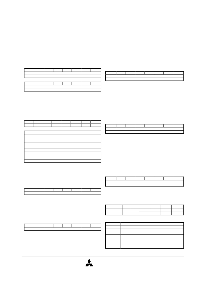
ATA Register Specifications
Data Register
This register is a 16 bit register which is used to transfer
data blocks between the card data buffer and the host.
Data may be transferred by either a series of word
accesses to the Data register or a series of byte accesses
to the Data register.
D15
D14
D13
D12
Data Word
Odd Data Byte
D11
D10
D9
D8
D7
D6
D5
D4
Data Word
Data Byte
D3
D2
D1
D0
Error Register
This register contains additional information about the
source of an error which has occurred in processing of the
preceding command. This register should be checked by
the host when ERR bit in the Status register is set. The
Error register is a read only register.
D7
BBK
D6
UNC
D5
0
D4
IDNF
D3
0
D2
D1
0
D0
ABRT
AMNF
Field
BBK
function
This bit is set when a Bad Block is detected in requested ID
field. Host can not read/write on data area that is marked as
a Bad Block.
This bit is set when Uncorrectable error is occurred at
reading the card.
The requested sector ID is in error or cannot be found.
This bit is set if the command has been aborted because of
the card status condition. (Not ready, Write fault, etc.) or
when an invalid command has been issued.
This bit is set in case of a general error.
UNC
IDNF
ABRT
AMNF
Feature Register
This register is written by the host to provide command
specific information to the drive regarding features of the
drive which the host wish to utilize. The Feature register is
a write only register.
D7
D6
D5
D4
Feature byte
D3
D2
D1
D0
Sector Count Register
This register is written by the host with the number of
sectors or blocks to be processed in the subsequent
command. After the command is complete, the host may
read this register to obtain the count of sectors left
unprocessed by the command.
D7
D6
D5
D4
Sector Count
D3
D2
D1
D0
Sector Number Register
This register is written by the host with the starting sector
number to be used in the subsequent Cylinder-Head-
Sector command. After the command is complete, the
host may read the final sector number from this register.
When logical block addressing is used, this register is
written by the host with bit7 to 0 of the starting logical
block number and contains bit7 to 0 of the final logical
block number after the command is complete.
D7
D6
D5
D4
Sector Number
D3
D2
D1
D0
Logical Block Number bits A07-A00(LBA Addressing)
Cylinder Low Register
This register is written by the host with the low-order byte
of the starting cylinder address to be used in the
subsequent Cylinder-Head-Sector command. After the
command is complete, the host may read the low-order
byte of the final cylinder number from this register. When
logical block addressing is used, this register is written by
the host with bits15 to 8 of the starting logical block
number and contains bits15 to 8 of the final logical block
number after the command complete.
D7
D6
D5
D4
D3
D2
D1
D0
Cylinder Low Byte
Logical Block Number bits A15-A08(LBA Addressing)
Cylinder High Register
This register is written by the host with the high-order byte
of the starting cylinder address to be used in the
subsequent Cylinder-Head-Sector command. After the
command is complete, the host may read the high-order
byte of the final cylinder number from this register. When
logical block addressing is used, this register is written by
the host with bits 23 to 16 of the starting logical block
number and contains bits23 to 16 of the final logical block
number after the command is complete.
D7
D6
D5
D4
D3
D2
D1
D0
Cylinder High Byte
Logical Block Number bits A23-A16(LBA Addressing)
Drive/Head Register
The Drive/Head register is used to specify the selected
drive of a pair of drives sharing a set of registers.
D7
X
D6
LBA
D5
X
D4
DRV
D3
HS3
LBA27
D2
HS2
LBA26
D1
HS1
LBA25
D0
HS0
LBA24
Field
X
LBA
function
Undefined . “0” or “1”.
This bit is “0” for CHS addressing and “1” for Logical
Block addressing.
This bit is number of the drive which the host has
selected. When DRV is cleared, Drive0 is selected.
When DRV is set, Drive1 is selected. The card is
selected to be Drive0 or to be Drive1 using the “Copy”
field of the PC Card Socket Copy Register.
DRV
相关PDF资料 |
PDF描述 |
|---|---|
| MF0030M-03ATxx | null8/16-bit Data Bus Flash ATA PC Card |
| MF0045M-03ATxx | ER 26C 26#16 PIN RECP |
| MF0064M-04BAXX | 8/16-bit Data Bus CompactFlash Card |
| MF0064M-04AAxx | GT 10C 10#16 PIN PLUG |
| MF0064M-05AAxx | 8/16-bit Data Bus CompactFlash Card |
相关代理商/技术参数 |
参数描述 |
|---|---|
| MF0030M-03ATXX | 制造商:MITSUBISHI 制造商全称:Mitsubishi Electric Semiconductor 功能描述:null8/16-bit Data Bus Flash ATA PC Card |
| MF0032M-04AAXX | 制造商:MITSUBISHI 制造商全称:Mitsubishi Electric Semiconductor 功能描述:8/16-bit Data Bus CompactFlash Card |
| MF0032M-05AAXX | 制造商:MITSUBISHI 制造商全称:Mitsubishi Electric Semiconductor 功能描述:8/16-bit Data Bus CompactFlash Card |
| MF0032M-11ATXX | 制造商:MITSUBISHI 制造商全称:Mitsubishi Electric Semiconductor 功能描述:8/16-bit Data Bus Flash ATA PC Card |
| MF0040 | 功能描述:安装硬件 MOUNTING FEET FOR RP SERIES RoHS:否 制造商:Harwin 类型:SMT Cable Clip 材料:Phosphor Bronze 安装孔大小: 长度:5 mm 外径: 内径: 厚度: 电镀:Tin 螺纹大小: |
发布紧急采购,3分钟左右您将得到回复。