- 您现在的位置:买卖IC网 > PDF目录382324 > MF10 (National Semiconductor Corporation) Universal Monolithic Dual Switched Capacitor Filter PDF资料下载
参数资料
| 型号: | MF10 |
| 厂商: | National Semiconductor Corporation |
| 英文描述: | Universal Monolithic Dual Switched Capacitor Filter |
| 中文描述: | 通用单片双开关电容滤波器 |
| 文件页数: | 13/20页 |
| 文件大小: | 405K |
| 代理商: | MF10 |
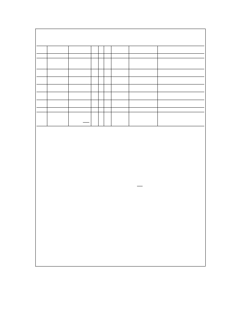
2.0 Modes of Operation
(Continued)
TABLE I. Summary of Modes. Realizable filter types (e.g. low-pass) denoted by asterisks.
Unless otherwise noted, gains of various filter outputs are inverting and adjustable by resistor ratios.
Mode
BP
LP
HP
N
AP
Number of
Resistors
Adjustable
f
CLK
/f
O
No
Notes
1
*
*
*
3
(2)
May need input buffer.
Poor dynamics for
high Q.
1a
H
OBP1
e b
Q
H
OBP2
e a
1
H
OLP
a
1
2
No
2
*
*
*
3
Yes (above f
CLK
/50
or f
CLK
/100)
3
*
*
*
4
Yes
Universal State-Variable
Filter. Best general-purpose mode.
3a
*
*
*
*
7
Yes
As above, but also includes
resistor-tuneable notch.
4
*
*
*
3
No
Gives Allpass response with
H
OAP
e b
1 and H
OLP
e b
2.
Gives flatter allpass response
than above if R
1
e
R
2
e
0.02R
4
.
Single pole.
5
*
*
*
4
6a
*
*
3
(2)
6b
H
OLP1
e a
1
H
OLP2
eb
R3
2
Single Pole.
R2
3.0 Applications Information
The MF10 is a general-purpose dual second-order state
variable filter whose center frequency is proportional to the
frequency of the square wave applied to the clock input
(f
CLK
). By connecting pin 12 to the appropriate DC voltage,
the filter center frequency f
O
can be made equal to either
f
CLK
/100 or f
CLK
/50. f
O
can be very accurately set (within
g
6%) by using a crystal clock oscillator, or can be easily
varied over a wide frequency range by adjusting the clock
frequency. If desired, the f
CLK
/f
O
ratio can be altered by
external resistors as inFigures 9, 10, 11, 13, 14 and15. The
filter Q and gain are determined by external resistors.
All of the five second-order filter types can be built using
either section of the MF10. These are illustrated inFigures 1
through5 along with their transfer functions and some relat-
ed equations.Figure 6 shows the effect of Q on the shapes
of these curves. When filter orders greater than two are
desired, two or more MF10 sections can be cascaded.
3.1 DESIGN EXAMPLE
In order to design a second-order filter section using the
MF10, we must define the necessary values of three param-
eters: f
0
, the filter section’s center frequency; H
0
, the pass-
band gain; and the filter’s Q. These are determined by the
characteristics required of the filter being designed.
As an example, let’s assume that a system requires a
fourth-order Chebyshev low-pass filter with 1 dB ripple, unity
gain at DC, and 1000 Hz cutoff frequency. As the system
order is four, it is realizable using both second-order sec-
tions of an MF10. Many filter design texts include tables that
list the characteristics (f
O
and Q) of each of the second-or-
der filter sections needed to synthesize a given higher-order
filter. For the Chebyshev filter defined above, such a table
yields the following characteristics:
f
0A
e
529 Hz
Q
A
e
0.785
f
0B
e
993 Hz
Q
B
e
3.559
For unity gain at DC, we also specify:
H
0A
e
1
H
0B
e
1
The desired clock-to-cutoff-frequency ratio for the overall
filter of this example is 100 and a 100 kHz clock signal is
available. Note that the required center frequencies for the
two second-order sections will not be obtainable with clock-
to-center-frequency ratios of 50 or 100. It will be necessary
to adjustf
CLK
f
0
externally. From Table I, we see that Mode 3
can be used to produce a low-pass filter with resistor-adjust-
able center frequency.
In most filter designs involving multiple second-order
stages, it is best to place the stages with lower Q values
ahead of stages with higher Q, especially when the higher Q
is greater than 0.707. This is due to the higher relative gain
at the center frequency of a higher-Q stage. Placing a stage
with lower Q ahead of a higher-Q stage will provide some
attenuation at the center frequency and thus help avoid clip-
ping of signals near this frequency. For this example, stage
A has the lower Q (0.785) so it will be placed ahead of the
other stage.
For the first section, we begin the design by choosing a
convenient value for the input resistance: R
1A
e
20k. The
absolute value of the passband gain H
OLPA
is made equal
13
相关PDF资料 |
PDF描述 |
|---|---|
| MF10ACN | Universal Monolithic Dual Switched Capacitor Filter |
| MF10ACWM | Universal Monolithic Dual Switched Capacitor Filter |
| MF4CN-100 | 4TH ORDER SWITCHED CAPACITOR BUTTERWORTH |
| MF4CN-50 | 4TH ORDER SWITCHED CAPACITOR BUTTERWORTH |
| MF4CWM-100 | 4TH ORDER SWITCHED CAPACITOR BUTTERWORTH |
相关代理商/技术参数 |
参数描述 |
|---|---|
| MF10.7-12B | 制造商:ECS 制造商全称:ECS, Inc. 功能描述:MONOLITHIC CRYSTAL FILTERS |
| MF10.7-12C | 制造商:ECS 制造商全称:ECS, Inc. 功能描述:MONOLITHIC CRYSTAL FILTERS |
| MF10.7-12D | 制造商:ECS 制造商全称:ECS, Inc. 功能描述:MONOLITHIC CRYSTAL FILTERS |
| MF10/CVMD | 制造商:Hirose 功能描述:902-6056-4-00 EACH 制造商:Hirose 功能描述:MF10/CVMD |
| MF10/CVMD2 | 制造商:Hirose 功能描述:902-6060-1-00 EACH 制造商:Hirose 功能描述:MF10/CVMD2 |
发布紧急采购,3分钟左右您将得到回复。