- 您现在的位置:买卖IC网 > PDF目录382324 > MF10ACWM (NATIONAL SEMICONDUCTOR CORP) Universal Monolithic Dual Switched Capacitor Filter PDF资料下载
参数资料
| 型号: | MF10ACWM |
| 厂商: | NATIONAL SEMICONDUCTOR CORP |
| 元件分类: | 运动控制电子 |
| 英文描述: | Universal Monolithic Dual Switched Capacitor Filter |
| 中文描述: | SWITCHED CAPACITOR FILTER, BUTTERWORTH/BESSEL/CHEBYSHEV, UNIVERSAL, PDSO20 |
| 封装: | PLASTIC, SO-20 |
| 文件页数: | 3/20页 |
| 文件大小: | 405K |
| 代理商: | MF10ACWM |
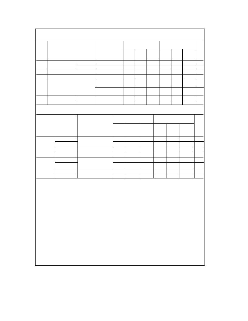
Electrical Characteristics
(Continued) V
a
e a
5.00V and V
b
e b
5.00V unless otherwise specified.
Boldface limits apply for T
MIN
to T
MAX
;
all other limits T
A
e
T
J
e
25
§
C.
MF10ACN, MF10CCN,
MF10ACWM, MF10CCWM
MF10CCJ, MF10AJ
Symbol
Parameter
Conditions
Typical
(Note 8)
Tested
Limit
(Note 9) (Note 10)
Design
Limit
Typical
(Note 8)
Tested
Limit
(Note 9) (Note 10)
Design Units
Limit
V
OUT
Minimum Output
Voltage Swing
BP, LP Pins
R
L
e
5k
g
4.25
g
3.8
g
3.8
g
4.25
g
3.8
V
N/AP/HP Pin R
L
e
3.5k
g
4.25
g
3.8
g
3.8
g
4.25
g
3.6
V
GBW
Op Amp Gain BW Product
2.5
2.5
MHz
SR
Op Amp Slew Rate
7
7
V/
m
s
Dynamic Range
(Note 6)
V
pin12
e a
5V
(f
CLK
/f
O
e
50)
V
pin12
e
0V
(f
CLK
/f
O
e
100)
83
83
dB
80
80
dB
I
SC
Maximum Output Short Source
Circuit Current (Note 7)Sink
20
20
mA
3.0
3.0
mA
Logic Input Characteristics
Boldface limits apply for T
MIN
to T
MAX
;
all other limits T
A
e
T
J
e
25
§
C
MF10ACN, MF10CCN,
MF10ACWM, MF10CCWM
MF10CCJ, MF10AJ
Parameter
Conditions
Typical
(Note 8)
Tested
Limit
(Note 9) (Note 10)
Design
Limit
Typical
(Note 8)
Tested
Limit
(Note 9) (Note 10)
Design
Limit
Units
CMOS Clock
Input Voltage
Min Logical ‘‘1’’
V
a
e a
5V, V
b
e b
5V,
V
LSh
e
0V
a
3.0
a
3.0
a
3.0
V
Max Logical ‘‘0’’
b
3.0
b
3.0
b
3.0
V
Min Logical ‘‘1’’
V
a
e a
10V, V
b
e
0V,
V
LSh
e a
5V
a
8.0
a
8.0
a
8.0
V
Max Logical ‘‘0’’
a
2.0
a
2.0
a
2.0
V
TTL Clock
Input Voltage
Min Logical ‘‘1’’
V
a
e a
5V, V
b
e b
5V,
V
LSh
e
0V
a
2.0
a
2.0
a
2.0
V
Max Logical ‘‘0’’
a
0.8
a
0.8
a
0.8
V
Min Logical ‘‘1’’
V
a
e a
10V, V
b
e
0V,
V
LSh
a
2.0
a
2.0
a
2.0
V
Max Logical ‘‘0’’
a
0.8
a
0.8
a
0.8
V
Note 1:
Absolute Maximum Ratings indicate limits beyond which damage to the device may occur. DC and AC electrical specifications do not apply when operating
the device beyond its specified operating conditions.
Note 2:
When the input voltage (V
IN
) at any pin exceeds the power supply rails (V
IN
k
V
b
or V
IN
l
V
a
) the absolute value of current at that pin should be limited
to 5 mA or less. The 20 mA package input current limits the number of pins that can exceed the power supply boundaries with a 5 mA current limit to four.
Note 3:
The maximum power dissipation must be derated at elevated temperatures and is dictated by T
JMAX
,
i
JA
, and the ambient temperature, T
A
. The maximum
allowable power dissipation at any temperature is P
D
e
(T
JMAX
b
T
A
)/
i
JA
or the number given in the Absolute Maximum Ratings, whichever is lower. For this
device, T
JMAX
e
125
§
C, and the typical junction-to-ambient thermal resistance of the MF10ACN/CCN when board mounted is 55
§
C/W. For the MF10AJ/CCJ, this
number increases to 95
§
C/W and for the MF10ACWM/CCWM this number is 66
§
C/W.
Note 4:
The accuracy of the Q value is a function of the center frequency (f
O
). This is illustrated in the curves under the heading ‘‘Typical Performance
Characteristics’’.
Note 5:
V
OS1
, V
OS2
, and V
OS3
refer to the internal offsets as discussed in the Applications Information Section 3.4.
Note 6:
For
g
5V supplies the dynamic range is referenced to 2.82V rms (4V peak) where the wideband noise over a 20 kHz bandwidth is typically 200
m
V rms for
the MF10 with a 50:1 CLK ratio and 280
m
V rms for the MF10 with a 100:1 CLK ratio.
Note 7:
The short circuit source current is measured by forcing the output that is being tested to its maximum positive voltage swing and then shorting that output to
the negative supply. The short circuit sink current is measured by forcing the output that is being tested to its maximum negative voltage swing and then shorting
that output to the positive supply. These are the worst case conditions.
Note 8:
Typicals are at 25
§
C and represent most likely parametric norm.
Note 9:
Tested limits are guaranteed to National’s AOQL (Average Outgoing Quality Level).
Note 10:
Design limits are guaranteed but not 100% tested. These limits are not used to calculate outgoing quality levels.
Note 11:
Human body model, 100 pF discharged through a 1.5 k
X
resistor.
3
相关PDF资料 |
PDF描述 |
|---|---|
| MF4CN-100 | 4TH ORDER SWITCHED CAPACITOR BUTTERWORTH |
| MF4CN-50 | 4TH ORDER SWITCHED CAPACITOR BUTTERWORTH |
| MF4CWM-100 | 4TH ORDER SWITCHED CAPACITOR BUTTERWORTH |
| MF4CWM-50 | 4TH ORDER SWITCHED CAPACITOR BUTTERWORTH |
| MF4 | MF4 4th Order Switched Capacitor Butterworth Lowpass Filter |
相关代理商/技术参数 |
参数描述 |
|---|---|
| MF10AJ | 制造商:Rochester Electronics LLC 功能描述:- Bulk |
| MF10BJ | 功能描述:有源滤波器 RoHS:否 制造商:Maxim Integrated 通道数量:1 截止频率:150 KHz 电源电压-最大:11 V 电源电压-最小:4.74 V 最大工作温度:+ 85 C 安装风格:Through Hole 封装 / 箱体:PDIP N 封装:Tube |
| MF10BN | 功能描述:有源滤波器 RoHS:否 制造商:Maxim Integrated 通道数量:1 截止频率:150 KHz 电源电压-最大:11 V 电源电压-最小:4.74 V 最大工作温度:+ 85 C 安装风格:Through Hole 封装 / 箱体:PDIP N 封装:Tube |
| MF10BN+ | 功能描述:有源滤波器 RoHS:否 制造商:Maxim Integrated 通道数量:1 截止频率:150 KHz 电源电压-最大:11 V 电源电压-最小:4.74 V 最大工作温度:+ 85 C 安装风格:Through Hole 封装 / 箱体:PDIP N 封装:Tube |
| MF10BWP | 功能描述:有源滤波器 RoHS:否 制造商:Maxim Integrated 通道数量:1 截止频率:150 KHz 电源电压-最大:11 V 电源电压-最小:4.74 V 最大工作温度:+ 85 C 安装风格:Through Hole 封装 / 箱体:PDIP N 封装:Tube |
发布紧急采购,3分钟左右您将得到回复。