- 您现在的位置:买卖IC网 > PDF目录382324 > MF10CCJ (NATIONAL SEMICONDUCTOR CORP) Universal Monolithic Dual Switched Capacitor Filter PDF资料下载
参数资料
| 型号: | MF10CCJ |
| 厂商: | NATIONAL SEMICONDUCTOR CORP |
| 元件分类: | 运动控制电子 |
| 英文描述: | Universal Monolithic Dual Switched Capacitor Filter |
| 中文描述: | DUAL SWITCHED CAPACITOR FILTER, RESISTOR PROGRAMMABLE, UNIVERSAL, CDIP20 |
| 封装: | 0.300 INCH, CERAMIC, DIP-20 |
| 文件页数: | 15/20页 |
| 文件大小: | 405K |
| 代理商: | MF10CCJ |
3.0 Applications Information
(Continued)
TL/H/10399–27
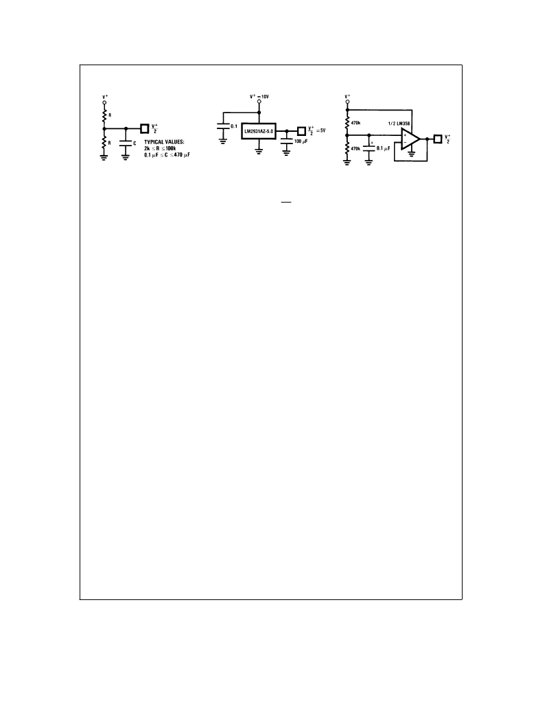
(a) Resistive Divider with
Decoupling Capacitor
TL/H/10399–28
(b) Voltage Regulator
TL/H/10399–29
(c) Operational Amplifier
with Divider
FIGURE 18. Three Ways of GeneratingV
a
2
for Single-Supply Operation
3.2 SINGLE SUPPLY OPERATION
The MF10 can also operate with a single-ended power sup-
ply. Figure 17 shows the example filter with a single-ended
power supply. V
A
a
and V
D
a
are again connected to the
positive power supply (8V to 14V), and V
A
b
and V
D
b
are
connected to ground. The A
GND
pin must be tied to V
a
/2
for single supply operation. This half-supply point should be
very ‘‘clean’’, as any noise appearing on it will be treated as
an input to the filter. It can be derived from the supply volt-
age with a pair of resistors and a bypass capacitor (Figure
18a), or a low-impedance half-supply voltage can be made
using a three-terminal voltage regulator or an operational
amplifier(Figures 18b and18c). The passive resistor divider
with a bypass capacitor is sufficient for many applications,
provided that the time constant is long enough to reject any
power supply noise. It is also important that the half-supply
reference present a low impedance to the clock frequency,
so at very low clock frequencies the regulator or op-amp
approaches may be preferable because they will require
smaller capacitors to filter the clock frequency. The main
power supply voltage should be clean (preferably regulated)
and bypassed with 0.1
m
F.
3.3 DYNAMIC CONSIDERATIONS
The maximum signal handling capability of the MF10, like
that of any active filter, is limited by the power supply volt-
ages used. The amplifiers in the MF10 are able to swing to
within about 1V of the supplies, so the input signals must be
kept small enough that none of the outputs will exceed
these limits. If the MF10 is operating on
g
5V, for example,
the outputs will clip at about 8 V
p–p
. The maximum input
voltage multiplied by the filter gain should therefore be less
than 8 V
p–p
.
Note that if the filter Q is high, the gain at the lowpass or
highpass outputs will be much greater than the nominal filter
gain (Figure 6). As an example, a lowpass filter with a Q of
10 will have a 20 dB peak in its amplitude response at f
O
. If
the nominal gain of the filter H
OLP
is equal to 1, the gain at
f
O
will be 10. The maximum input signal at f
O
must therefore
be less than 800 mV
p–p
when the circuit is operated on
g
5V supplies.
Also note that one output can have a reasonable small volt-
age on it while another is saturated. This is most likely for a
circuit such as the notch in Mode 1 (Figure 7). The notch
output will be very small at f
O
, so it might appear safe to
apply a large signal to the input. However, the bandpass will
have its maximum gain at f
O
and can clip if overdriven. If
one output clips, the performance at the other outputs will
be degraded, so avoid overdriving any filter section, even
ones whose outputs are not being directly used. Accompa-
nying Figures 7 through 15 are equations labeled ‘‘circuit
dynamics’’, which relate the Q and the gains at the various
outputs. These should be consulted to determine peak cir-
cuit gains and maximum allowable signals for a given appli-
cation.
3.4 OFFSET VOLTAGE
The MF10’s switched capacitor integrators have a higher
equivalent input offset voltage than would be found in a
typical continuous-time active filter integrator. Figure 19
shows an equivalent circuit of the MF10 from which the out-
put DC offsets can be calculated. Typical values for these
offsets with S
A/B
tied to V
a
are:
V
os1
e
opamp offset
e
g
5 mV
V
os2
e b
150 mV
@
50:1
V
os3
e b
70 mV
@
50:1
When S
A/B
is tied to V
b
, V
os2
will approximately halve. The
DC offset at the BP output is equal to the input offset of the
lowpass integrator (V
os3
). The offsets at the other outputs
depend on the mode of operation and the resistor ratios, as
described in the following expressions.
b
300 mV
@
100:1
b
140 mV
@
100:1
15
相关PDF资料 |
PDF描述 |
|---|---|
| MF10 | Universal Monolithic Dual Switched Capacitor Filter |
| MF10ACN | Universal Monolithic Dual Switched Capacitor Filter |
| MF10ACWM | Universal Monolithic Dual Switched Capacitor Filter |
| MF4CN-100 | 4TH ORDER SWITCHED CAPACITOR BUTTERWORTH |
| MF4CN-50 | 4TH ORDER SWITCHED CAPACITOR BUTTERWORTH |
相关代理商/技术参数 |
参数描述 |
|---|---|
| MF10CCN | 功能描述:有源滤波器 RoHS:否 制造商:Maxim Integrated 通道数量:1 截止频率:150 KHz 电源电压-最大:11 V 电源电压-最小:4.74 V 最大工作温度:+ 85 C 安装风格:Through Hole 封装 / 箱体:PDIP N 封装:Tube |
| MF10CCN | 制造商:Texas Instruments 功能描述:IC FILTER DUAL SWITCHED CAP DIP20 |
| MF10CCN/NOPB | 功能描述:有源滤波器 Univ Mono Dual Switched Cap Filter RoHS:否 制造商:Maxim Integrated 通道数量:1 截止频率:150 KHz 电源电压-最大:11 V 电源电压-最小:4.74 V 最大工作温度:+ 85 C 安装风格:Through Hole 封装 / 箱体:PDIP N 封装:Tube |
| MF10CCN/NOPB | 制造商:Texas Instruments 功能描述:Active Analog Filter IC |
| MF10CCWM | 功能描述:有源滤波器 RoHS:否 制造商:Maxim Integrated 通道数量:1 截止频率:150 KHz 电源电压-最大:11 V 电源电压-最小:4.74 V 最大工作温度:+ 85 C 安装风格:Through Hole 封装 / 箱体:PDIP N 封装:Tube |
发布紧急采购,3分钟左右您将得到回复。