- 您现在的位置:买卖IC网 > PDF目录382324 > MF5CWM (NATIONAL SEMICONDUCTOR CORP) MF5 Universal Monolithic Switched Capacitor Filter PDF资料下载
参数资料
| 型号: | MF5CWM |
| 厂商: | NATIONAL SEMICONDUCTOR CORP |
| 元件分类: | 运动控制电子 |
| 英文描述: | MF5 Universal Monolithic Switched Capacitor Filter |
| 中文描述: | SWITCHED CAPACITOR FILTER, RESISTOR PROGRAMMABLE, UNIVERSAL, PDSO14 |
| 封装: | SO-14 |
| 文件页数: | 13/16页 |
| 文件大小: | 293K |
| 代理商: | MF5CWM |
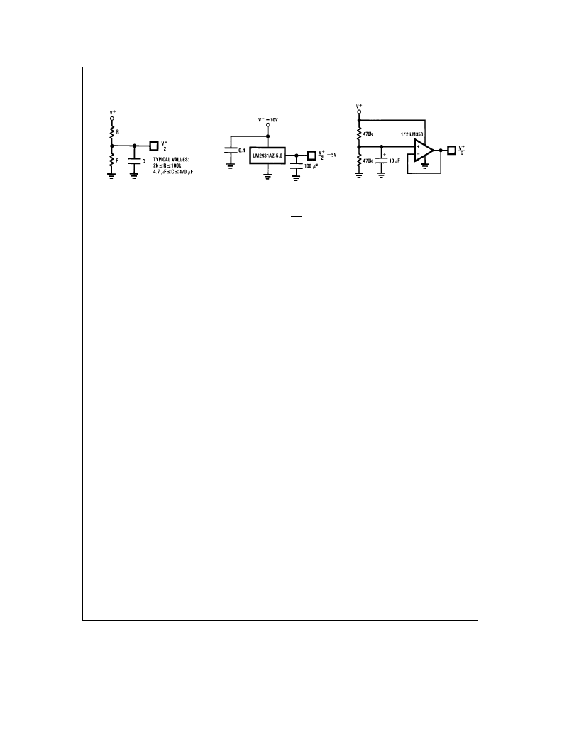
3.0 Applications Information
(Continued)
TL/H/5066–27
(a) Resistive Divider with
Decoupling Capaciter
TL/H/5066–28
(b) Voltage Regulator
TL/H/5066–29
(c) Operational Amplifier
with Divider
FIGURE 18. Three Ways of GeneratingV
a
2
for Single-supply Operation
For a cutoff frequency of 200 Hz, the external clock can be
either 10 kHz with pin 9 connected to V
a
(50:1) or 20 kHz
with pin 9 tied to A
GND
or V
b
(100:1). The voltage on the
Logic Level Shift pin (7) determines the logic threshold for
the clock input. The threshold is approximately 2V higher
than the voltage applied to pin 7. Therefore, when pin 7 is
grounded, the clock logic threshold will be 2V, making it
compatible with 0–5 volt TTL logic levels and
g
5 volt
CMOS levels. Pin 7 should be connected to a clean, low-im-
pedance (less than 1000
X
) voltage source.
The complete circuit of the design example is shown for a
100:1 clock ratio in Figure 16.
3.2 SINGLE SUPPLY OPERATION
The MF5 can also operate with a single-ended power sup-
ply. Figure 17 shows the example filter with a single-ended
power supply. V
a
is again connected to the positive power
supply (8 to 14 volts), and V
b
is connected to ground. The
A
GND
pin must be tied to V
a
/2 for single supply operation.
This half-supply point should be very ‘‘clean’’, as any noise
appearing on it will be treated as an input to the filter. It can
be derived from the supply voltage with a pair of resistors
and a bypass capacitor (Figure 18a), or a low-impedance
half-supply voltage can be made using a three-terminal volt-
age regulator or an operational amplifier (Figures 18b and
18c). The passive resistor divider with a bypass capacitor is
sufficient for many applications, provided that the time con-
stant is long enough to reject any power supply noise. It is
also important that the half-supply reference present a low
impedance to the clock frequency, so at very low clock fre-
quencies the regulator or op-amp approaches may be pref-
erable because they will require smaller capacitors to filter
the clock frequency. The main power supply voltage should
be clean (preferably regulated) and bypassed with 0.1
m
F.
3.3 DYNAMIC CONSIDERATIONS
The maximum signal handling capability of the MF5, like
that of any active filter, is limited by the power supply volt-
ages used. The amplifiers in the MF5 are able to swing to
within about 1 volt of the supplies, so the input signals must
be kept small enough that none of the outputs will exceed
these limits. If the MF5 is operating on
g
5 volts, for exam-
ple, the outputs will clip at about 8V
p-p
. The maximum input
voltage multiplied by the filter gain should therefore be less
than 8V
p-p
.
Note that if the filter has high Q, the gain at the lowpass or
highpass outputs will be much greater than the nominal filter
gain (Figure 6). As an example, a lowpass filter with a Q of
10 will have a 20 dB peak in its amplitude response at f
o
. If
the nominal gain of the filter H
OLP
is equal to 1, the gain at
f
o
will be 10. The maximum input signal at f
o
must therefore
be less than 800 mV
p-p
when the circuit is operated on
g
5
volt supplies.
Also note that one output can have a reasonable small volt-
age on it while another is saturated. This is most likely for a
circuit such as the notch in Mode 1 (Figure 7). The notch
output will be very small at f
o
, so it might appear safe to
apply a large signal to the input. However, the bandpass will
have its maximum gain at f
o
and can clip if overdriven. If one
output clips, the performance at the other outputs will be
degraded, so avoid overdriving any filter section, even ones
whose outputs are not being directly used. Accompanying
Figures 7 through 15 are equations labeled ‘‘circuit dynam-
ics’’, which relate the Q and the gains at the various outputs.
These should be consulted to determine peak circuit gains
and maximum allowable signals for a given application.
3.4 OFFSET VOLTAGE
The MF5’s switched capacitor integrators have a higher
equivalent input offset voltage than would be found in a
typical continuous-time active filter integrator. Figure 19
shows an equivalent circuit of the MF5 from which the out-
put dc offsets can be calculated. Typical values for these
offsets are:
V
os1
e
opamp offset
e
g
5mV
V
os2
e b
185mV
@
50:1
V
os3
e a
115mV
@
50:1
The dc offset at the BP output is equal to the input offset of
the lowpass integrator (V
os3
). The offsets at the other out-
puts depend on the mode of operation and the resistor ra-
tios, as described in the following expressions.
b
310mV
@
100:1
a
240mV
@
100:1
13
相关PDF资料 |
PDF描述 |
|---|---|
| MF600SWI | Mirco Filter For ADSL CPE Side |
| MF601F | Mirco Filter For ADSL CPE Side |
| MF602F | Mirco Filter For ADSL CPE Side |
| MF609 | The in-Line Micro filter |
| MF609A | The in-Line Micro filter |
相关代理商/技术参数 |
参数描述 |
|---|---|
| MF6 | 制造商:NSC 制造商全称:National Semiconductor 功能描述:6th Order Switched Capacitor Butterworth Lowpass |
| MF6. 3FD101MD13TP | 制造商:nippon chemicon 功能描述: |
| MF6.3FC101MD13TP | 制造商:UCC 功能描述: 制造商:United Chemi-Con Inc 功能描述: |
| MF6.3FC22RMD6TP | 制造商:United Chemi-Con Inc 功能描述: |
| MF60 | 制造商:RIEDON 制造商全称:Riedon Powertron 功能描述:Film Resistors |
发布紧急采购,3分钟左右您将得到回复。