- 您现在的位置:买卖IC网 > PDF目录382324 > MF6CWM-50 (NATIONAL SEMICONDUCTOR CORP) 6th Order Switched Capacitor Butterworth Lowpass PDF资料下载
参数资料
| 型号: | MF6CWM-50 |
| 厂商: | NATIONAL SEMICONDUCTOR CORP |
| 元件分类: | 运动控制电子 |
| 英文描述: | 6th Order Switched Capacitor Butterworth Lowpass |
| 中文描述: | SWITCHED CAPACITOR FILTER, BUTTERWORTH, LOWPASS, PDSO14 |
| 封装: | SO-14 |
| 文件页数: | 13/20页 |
| 文件大小: | 861K |
| 代理商: | MF6CWM-50 |
1.0 MF6 Application Hints
(Continued)
Schmitt-trigger threshold voltage levels can change signifi-
cantly causing the R/C oscillator’s frequency to vary greatly
from part to part.
Where accuracy in f
is required an external clock can be
used to drive the CLK R input of the MF6. This input is TTL
logic level compatible and also presents a very light load to
the external clock source (
z
2 μA) with split supplies and
L. Sh tied to system ground. The logic level is programmed
by the voltage applied to level shift (L. Sh) pin (See the Pin
description for L. Sh pin).
1.2 POWER SUPPLY BIASING
The MF6 can be biased from a single supply or dual split
supplies. The split supply mode shown in Figure 2 and Fig-
ure 3 is the most flexible and easiest to implement. As dis-
cussed earlier split supplies,
±
5V to
±
7V, will enable the use
of TTL or CMOS clock logic levels. Figure 4 shows two
schemes for single supply biasing. In this mode only CMOS
clock logic levels can be used.
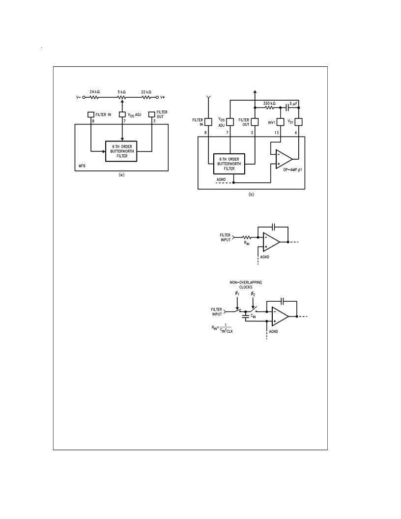
1.3 OFFSET ADJUST
The VosADJ pin is used in adjusting the output offset level of
the filter section. If this pin is not used it must be tied to the
analog ground (AGND) level, either mid-supply for single
ended supply operation or ground for split supply operation.
This pin sets the zero reference for the output of the filter.
The implementation of this pin can be seen in Figure 5 In
Figure 5a DC offset is adjusted using a potentiometer; in
Figure 5b the Op-Amp integrator circuit keeps the average
DC output level atAGND. The circuit in Figure 5bis therefore
appropriate only for AC-coupled signals and signals biased
at AGND.
1.4 INPUT IMPEDANCE
The MF6 lowpass filter input (FILTER IN pin) is not a high im-
pedance buffer input. This input is a switched capacitor re-
sistor equivalent, and its effective impedance is inversely
proportional to the clock frequency. The equivalent circuit of
the input to the filter can be seen in Figure 6 The input ca-
pacitor charges to the input voltage (V
) during one half of
the clock period, during the second half the charge is trans-
ferred to the feedback capacitor. The total transfer of charge
in one clock cycle is therefore Q = C
V
, and since current
is defined as the flow of charge per unit time the average in-
put current becomes
I
in
= Q/T
DS005065-16
DS005065-17
FIGURE 5. V
OS
Adjust Schemes
DS005065-18
a) Equivalent Circuit for MF6 Filter Input
DS005065-19
b) Actual Circuit for MF6 Filter Input
FIGURE 6. MF6 Filter Input
www.national.com
13
相关PDF资料 |
PDF描述 |
|---|---|
| MF6C | ORDER SWITCHED CAPACITOR BUTTERWORTH LOWPASS FILTER |
| MF6 | 6th Order Switched Capacitor Butterworth Lowpass |
| MFE1842BBU22 | Dielectric Filter with Attenuation Pole |
| MG-12232-3 | LCD MODULE |
| MG-12232-5 | LCD MODULE |
相关代理商/技术参数 |
参数描述 |
|---|---|
| MF6M | 制造商:GOOD-ARK 制造商全称:GOOD-ARK Electronics 功能描述:Miniature Glass Passivated Single-Phase Bridge Rectifiers |
| MF6S | 制造商:GOOD-ARK 制造商全称:GOOD-ARK Electronics 功能描述:Miniature Glass Passivated Single-Phase Bridge Rectifiers |
| MF-7 | 制造商:Velleman Inc 功能描述:Conn Power Adapter M/F 2/2 POS ST 1 Port Bulk |
| MF70 | 制造商:DYNEX 制造商全称:Dynex Semiconductor 功能描述:Fast Recovery Diode |
| MF-70 | 制造商:COOPER INDUSTRIES 功能描述:UNV WRNCH STANDARD 1/2 FMALE S |
发布紧急采购,3分钟左右您将得到回复。