- 您现在的位置:买卖IC网 > PDF目录15115 > MIC2182-5.0BSM TR (Micrel Inc)IC REG CTRLR BUCK PWM CM 16-SSOP PDF资料下载
参数资料
| 型号: | MIC2182-5.0BSM TR |
| 厂商: | Micrel Inc |
| 文件页数: | 18/28页 |
| 文件大小: | 0K |
| 描述: | IC REG CTRLR BUCK PWM CM 16-SSOP |
| 标准包装: | 1,000 |
| PWM 型: | 电流模式 |
| 输出数: | 1 |
| 频率 - 最大: | 330kHz |
| 占空比: | 86% |
| 电源电压: | 4.5 V ~ 32 V |
| 降压: | 是 |
| 升压: | 无 |
| 回扫: | 无 |
| 反相: | 无 |
| 倍增器: | 无 |
| 除法器: | 无 |
| Cuk: | 无 |
| 隔离: | 无 |
| 工作温度: | -40°C ~ 85°C |
| 封装/外壳: | 16-SSOP(0.209",5.30mm 宽) |
| 包装: | 带卷 (TR) |
| 其它名称: | MIC2182-5.0BSMTR MIC2182-5.0BSMTR-ND |
第1页第2页第3页第4页第5页第6页第7页第8页第9页第10页第11页第12页第13页第14页第15页第16页第17页当前第18页第19页第20页第21页第22页第23页第24页第25页第26页第27页第28页
�� �
�
�MIC2182�
�For� the� low-side� switch� (N-channel� MOSFET),� the� dc� power�
�dissipation� is:�
�P� switch2(dc)� =� R� DS(on)2� � I� SW� 2� (rms)� 2�
�Since� the� ac� switching� losses� for� the� low� side� MOSFET� is�
�near� zero,� the� total� power� dissipation� is:�
�P� low-side� MOSFET(max)� =� P� switch2(dc)�
�The� total� power� dissipation� for� the� high-side� MOSFET� is:�
�P� highsideMOSFET(max)� =� P� SWITCH� 1(dc)� +� P� AC�
�External� Schottky� Diode�
�An� external� freewheeling� diode� is� used� to� keep� the� inductor�
�current� flow� continuous� while� both� MOSFETs� are� turned� off.�
�This� dead� time� prevents� current� from� flowing� unimpeded�
�through� both� MOSFETs� and� is� typically� 80ns� The� diode�
�conducts� twice� during� each� switching� cycle.� Although� the�
�average� current� through� this� diode� is� small,� the� diode� must� be�
�able� to� handle� the� peak� current.�
�I� D(avg)� =� I� OUT� � 2� � 80ns� � f� S�
�Micrel�
�circuit� inductance� will� cause� ringing� during� the� high-side�
�MOSFET� turn-on.�
�An� external� Schottky� diode� conducts� at� a� lower� forward�
�voltage� preventing� the� body� diode� in� the� MOSFET� from�
�turning� on.� The� lower� forward� voltage� drop� dissipates� less�
�power� than� the� body� diode.� The� lack� of� a� reverse� recovery�
�mechanism� in� a� Schottky� diode� causes� less� ringing� and� less�
�power� loss.� Depending� on� the� circuit� components� and� oper-�
�ating� conditions,� an� external� Schottky� diode� will� give� a� 1/2%�
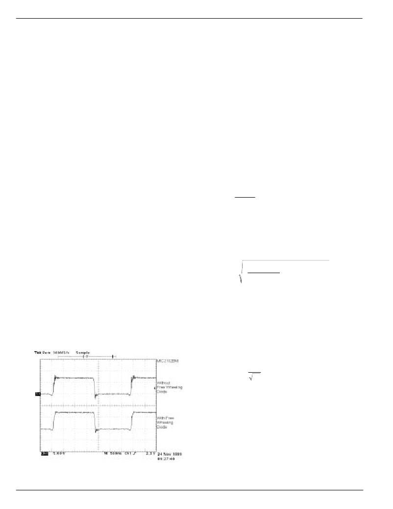
�to� 1%� improvement� in� efficiency.� Figure� 12� illustrates� the�
�difference� in� noise� on� the� VSW� pin� with� and� without� a�
�Schottky� diode.�
�Output� Capacitor� Selection�
�The� output� capacitor� values� are� usually� determined� by� the�
�capacitors� ESR� (equivalent� series� resistance).� Voltage� rating�
�and� RMS� current� capability� are� two� other� important� factors� in�
�selecting� the� output� capacitor.� Recommended� capacitors� are�
�tantalum,� low-ESR� aluminum� electrolytics,� and� OS-CON.�
�The� output� capacitor� ’� s� ESR� is� usually� the� main� cause� of�
�output� ripple.� The� maximum� value� of� ESR� is� calculated� by:�
�The� reverse� voltage� requirement� of� the� diode� is:�
�V� diode� (rrm)� =� V� IN�
�The� power� dissipated� by� the� Schottky� diode� is:�
�R� ESR� ≤�
�where:�
�?� V� OUT�
�I� PP�
�P� diode� =� I� D(avg)� � V� F�
�where:�
�V� F� =� forward� voltage� at� the� peak� diode� current�
�V� OUT� =� peak� to� peak� output� voltage� ripple�
�I� PP� =� peak� to� peak� inductor� ripple� current�
�The� total� output� ripple� is� a� combination� of� the� ESR� and� the�
�output� capacitance.� The� total� ripple� is� calculated� below:�
�The� external� Schottky� diode,� D2,� is� not� necessary� for� circuit�
�operation� since� the� low-side� MOSFET� contains� a� parasitic�
�body� diode.� The� external� diode� will� improve� efficiency� and�
�decrease� high� frequency� noise.� If� the� MOSFET� body� diode� is�
�?� V� OUT� =�
�?� I� PP� � (1� ?� D)� ?�
�?� ?�
�?� C� OUT� � f� S� ?�
�2�
�+� (� I� PP� � R� ESR�
�)� 2�
�used,� it� must� be� rated� to� handle� the� peak� and� average� current.�
�The� body� diode� has� a� relatively� slow� reverse� recovery� time�
�and� a� relatively� high� forward� voltage� drop.� The� power� lost� in�
�the� diode� is� proportional� to� the� forward� voltage� drop� of� the�
�diode.� As� the� high-side� MOSFET� starts� to� turn� on,� the� body�
�diode� becomes� a� short� circuit� for� the� reverse� recovery� period,�
�dissipating� additional� power.� The� diode� recovery� and� the�
�where:�
�D� =� duty� cycle�
�C� OUT� =� output� capacitance� value�
�f� S� =� switching� frequency�
�The� voltage� rating� of� capacitor� should� be� twice� the� output�
�voltage� for� a� tantalum� and� 20%� greater� for� an� aluminum�
�electrolytic� or� OS-CON.�
�The� output� capacitor� RMS� current� is� calculated� below:�
�I� C�
�OUT�
�(rms)� =�
�I� PP�
�12�
�The� power� dissipated� in� the� output� capacitor� is:�
�P� DISS(C�
�OUT� )�
�=� I� C�
�OUT�
�(rms)� 2� � R� ESR(C�
�OUT� )�
�Input� Capacitor� Selection�
�The� input� capacitor� should� be� selected� for� ripple� current�
�rating� and� voltage� rating.� Tantalum� input� capacitors� may� fail�
�when� subjected� to� high� inrush� currents,� caused� by� turning� the�
�input� supply� on.� Tantalum� input� capacitor� voltage� rating�
�TIME�
�Figure� 12.� Switch� Output� Noise�
�With� and� Without� Shottky� Diode�
�should� be� at� least� 2� times� the� maximum� input� voltage� to�
�maximize� reliability.� Aluminum� electrolytic,� OS-CON,� and�
�multilayer� polymer� film� capacitors� can� handle� the� higher�
�inrush� currents� without� voltage� derating.�
�M9999-042204�
�18�
�April� 22,� 2004�
�相关PDF资料 |
PDF描述 |
|---|---|
| MIC2182-5.0BSM | IC REG CTRLR BUCK PWM CM 16-SSOP |
| MIC2182-5.0BM TR | IC REG CTRLR BUCK PWM CM 16-SOIC |
| MIC2182-5.0BM | IC REG CTRLR BUCK PWM CM 16-SOIC |
| MIC2182-3.3BSM TR | IC REG CTRLR BUCK PWM CM 16-SSOP |
| MIC2182-3.3BSM | IC REG CTRLR BUCK PWM CM 16-SSOP |
相关代理商/技术参数 |
参数描述 |
|---|---|
| MIC2182BM | 功能描述:IC REG CTRLR BUCK PWM CM 16-SOIC RoHS:否 类别:集成电路 (IC) >> PMIC - 稳压器 - DC DC 切换控制器 系列:- 标准包装:4,000 系列:- PWM 型:电压模式 输出数:1 频率 - 最大:1.5MHz 占空比:66.7% 电源电压:4.75 V ~ 5.25 V 降压:是 升压:无 回扫:无 反相:无 倍增器:无 除法器:无 Cuk:无 隔离:无 工作温度:-40°C ~ 85°C 封装/外壳:40-VFQFN 裸露焊盘 包装:带卷 (TR) |
| MIC2182BM TR | 功能描述:IC REG CTRLR BUCK PWM CM 16-SOIC RoHS:否 类别:集成电路 (IC) >> PMIC - 稳压器 - DC DC 切换控制器 系列:- 标准包装:4,000 系列:- PWM 型:电压模式 输出数:1 频率 - 最大:1.5MHz 占空比:66.7% 电源电压:4.75 V ~ 5.25 V 降压:是 升压:无 回扫:无 反相:无 倍增器:无 除法器:无 Cuk:无 隔离:无 工作温度:-40°C ~ 85°C 封装/外壳:40-VFQFN 裸露焊盘 包装:带卷 (TR) |
| MIC2182BSM | 功能描述:DC/DC 开关控制器 High EfficiencySynchronous Buck Controller SSOP Pkg RoHS:否 制造商:Texas Instruments 输入电压:6 V to 100 V 开关频率: 输出电压:1.215 V to 80 V 输出电流:3.5 A 输出端数量:1 最大工作温度:+ 125 C 安装风格: 封装 / 箱体:CPAK |
| MIC2182BSM TR | 功能描述:DC/DC 开关控制器 High EfficiencySynchronous Buck Controller SSOP Pkg RoHS:否 制造商:Texas Instruments 输入电压:6 V to 100 V 开关频率: 输出电压:1.215 V to 80 V 输出电流:3.5 A 输出端数量:1 最大工作温度:+ 125 C 安装风格: 封装 / 箱体:CPAK |
| MIC2182BSMTR | 制造商:Rochester Electronics LLC 功能描述: 制造商:RF Micro Devices Inc 功能描述: |
发布紧急采购,3分钟左右您将得到回复。