- 您现在的位置:买卖IC网 > PDF目录15115 > MIC2182-5.0BSM (Micrel Inc)IC REG CTRLR BUCK PWM CM 16-SSOP PDF资料下载
参数资料
| 型号: | MIC2182-5.0BSM |
| 厂商: | Micrel Inc |
| 文件页数: | 19/28页 |
| 文件大小: | 0K |
| 描述: | IC REG CTRLR BUCK PWM CM 16-SSOP |
| 标准包装: | 77 |
| PWM 型: | 电流模式 |
| 输出数: | 1 |
| 频率 - 最大: | 330kHz |
| 占空比: | 86% |
| 电源电压: | 4.5 V ~ 32 V |
| 降压: | 是 |
| 升压: | 无 |
| 回扫: | 无 |
| 反相: | 无 |
| 倍增器: | 无 |
| 除法器: | 无 |
| Cuk: | 无 |
| 隔离: | 无 |
| 工作温度: | -40°C ~ 85°C |
| 封装/外壳: | 16-SSOP(0.209",5.30mm 宽) |
| 包装: | 管件 |
第1页第2页第3页第4页第5页第6页第7页第8页第9页第10页第11页第12页第13页第14页第15页第16页第17页第18页当前第19页第20页第21页第22页第23页第24页第25页第26页第27页第28页
�� �
�
�MIC2182�
�The� input� voltage� ripple� will� primarily� depend� on� the� input�
�capacitors� ESR.� The� peak� input� current� is� equal� to� the� peak�
�inductor� current,� so:�
�?� V� IN� =� I� inductor(peak)� � R� ESR(C� IN� )�
�The� input� capacitor� must� be� rated� for� the� input� current� ripple.�
�The� RMS� value� of� input� capacitor� current� is� determined� at� the�
�maximum� output� current.� Assuming� the� peak� to� peak� induc-�
�tor� ripple� current� is� low:�
�Micrel�
�?� Supply� current� to� the� MIC2182�
�?� MOSFET� gate-charge� power� (included� in� the� IC�
�supply� current)�
�?� Core� losses� in� the� output� inductor�
�To� maximize� efficiency� at� light� loads:�
�?� Use� a� low� gate-charge� MOSFET� or� use� the�
�smallest� MOSFET,� which� is� still� adequate� for�
�maximum� output� current.�
�I� C� IN� (rms)� ≈� I� OUT(max)� ×�
�D� � (1� ?� D)�
�?� Allow� the� MIC2182� to� run� in� skip� mode� at� lower�
�currents.�
�The� power� dissipated� in� the� input� capacitor� is:�
�P� DISS(C� IN� )� =� I� C� IN� (rms)� 2� � R� ESR(C� IN� )�
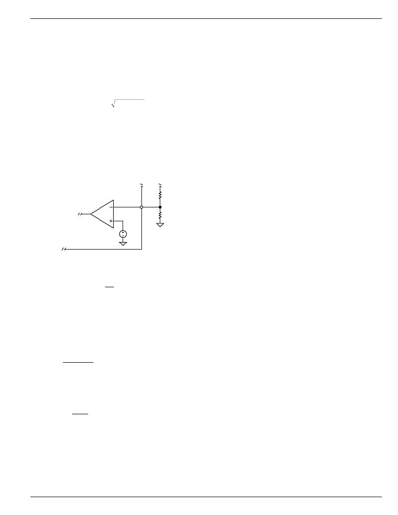
�Voltage� Setting� Components�
�The� MIC2182-3.3� and� MIC2182-5.0� ICs� contain� internal�
�voltage� dividers� that� set� the� output� voltage.� The� MIC2182�
�adjustable� version� requires� two� resistors� to� set� the� output�
�voltage� as� shown� in� Figure� 13.�
�?� Use� a� ferrite� material� for� the� inductor� core,� which�
�has� less� core� loss� than� an� MPP� or� iron� power�
�core.�
�Under� heavy� output� loads� the� significant� contributors� to�
�power� loss� are� (in� approximate� order� of� magnitude):�
�?� Resistive� on-time� losses� in� the� MOSFETs�
�?� Switching� transition� losses� in� the� MOSFETs�
�?� Inductor� resistive� losses�
�?� Current-sense� resistor� losses�
�Error�
�Amp�
�FB�
�7�
�R1�
�R2�
�?� Input� capacitor� resistive� losses� (due� to� the�
�capacitors� ESR)�
�To� minimize� power� loss� under� heavy� loads:�
�?� Use� logic-level,� low� on-resistance� MOSFETs.�
�MIC2182� [adj.]�
�V� REF�
�1.245V�
�Multiplying� the� gate� charge� by� the� on-resistance�
�gives� a� Figure� of� merit,� providing� a� good� bal-�
�ance� between� low� and� high� load� efficiency.�
�Figure� 13.� Voltage-Divider� Configuration�
�The� output� voltage� is� determined� by� the� equation:�
�?� Slow� transition� times� and� oscillations� on� the�
�voltage� and� current� waveforms� dissipate� more�
�power� during� turn-on� and� turnoff� of� the�
�V� O� =� V� REF� � ?� 1� +�
�?�
�?�
�?�
�R1� ?�
�R2� ?�
�MOSFETs.� A� clean� layout� will� minimize� parasitic�
�inductance� and� capacitance� in� the� gate� drive�
�Where:� V� REF� for� the� MIC2182� is� typically� 1.245V.�
�A� typical� value� of� R1� can� be� between� 3k� and� 10k.� If� R1� is� too�
�large� it� may� allow� noise� to� be� introduced� into� the� voltage�
�feedback� loop.� If� R1� is� too� small� in� value� it� will� decrease� the�
�efficiency� of� the� power� supply,� especially� at� low� output� loads.�
�Once� R1� is� selected,� R2� can� be� calculated� using:�
�and� high� current� paths.� This� will� allow� the� fastest�
�transition� times� and� waveforms� without� oscilla-�
�tions.� Low� gate-charge� MOSFETs� will� transition�
�faster� than� those� with� higher� gate-charge�
�requirements.�
�?� For� the� same� size� inductor,� a� lower� value� will�
�have� fewer� turns� and� therefore,� lower� winding�
�R2� =�
�V� REF� � R1�
�V� O� ?� V� REF�
�resistance.� However,� using� too� small� of� a� value�
�will� require� more� output� capacitors� to� filter� the�
�output� ripple,� which� will� force� a� smaller� band-�
�I� divider� =� REF�
�Voltage� Divider� Power� Dissipation�
�The� reference� voltage� and� R2� set� the� current� through� the�
�voltage� divider.�
�V�
�R2�
�The� power� dissipated� by� the� divider� resistors� is:�
�P� divider� =� (R1� +� R2)� � I� divider� 2�
�Efficiency� Calculation� and� Considerations�
�Efficiency� is� the� ratio� of� output� power� to� input� power.� The�
�difference� is� dissipated� as� heat� in� the� buck� converter.� Under�
�light� output� load,� the� significant� contributors� are:�
�width,� slower� transient� response� and� possible�
�instability� under� certain� conditions.�
�?� Lowering� the� current-sense� resistor� value� will�
�decrease� the� power� dissipated� in� the� resistor.�
�However,� it� will� also� increase� the� overcurrent�
�limit� and� will� require� larger� MOSFETs� and�
�inductor� components.�
�?� Use� low-ESR� input� capacitors� to� minimize� the�
�power� dissipated� in� the� capacitors� ESR.�
�Decoupling� Capacitor� Selection�
�The� 4.7� μ� F� decoupling� capacitor� is� used� to� minimize� noise� on�
�the� VDD� pin.� The� placement� of� this� capacitor� is� critical� to� the�
�proper� operation� of� the� IC.� It� must� be� placed� right� next� to� the�
�April� 22,� 2004�
�19�
�M9999-042204�
�相关PDF资料 |
PDF描述 |
|---|---|
| MIC2182-5.0BM TR | IC REG CTRLR BUCK PWM CM 16-SOIC |
| MIC2182-5.0BM | IC REG CTRLR BUCK PWM CM 16-SOIC |
| MIC2182-3.3BSM TR | IC REG CTRLR BUCK PWM CM 16-SSOP |
| MIC2182-3.3BSM | IC REG CTRLR BUCK PWM CM 16-SSOP |
| MIC2182-3.3BM TR | IC REG CTRLR BUCK PWM CM 16-SOIC |
相关代理商/技术参数 |
参数描述 |
|---|---|
| MIC2182BM | 功能描述:IC REG CTRLR BUCK PWM CM 16-SOIC RoHS:否 类别:集成电路 (IC) >> PMIC - 稳压器 - DC DC 切换控制器 系列:- 标准包装:4,000 系列:- PWM 型:电压模式 输出数:1 频率 - 最大:1.5MHz 占空比:66.7% 电源电压:4.75 V ~ 5.25 V 降压:是 升压:无 回扫:无 反相:无 倍增器:无 除法器:无 Cuk:无 隔离:无 工作温度:-40°C ~ 85°C 封装/外壳:40-VFQFN 裸露焊盘 包装:带卷 (TR) |
| MIC2182BM TR | 功能描述:IC REG CTRLR BUCK PWM CM 16-SOIC RoHS:否 类别:集成电路 (IC) >> PMIC - 稳压器 - DC DC 切换控制器 系列:- 标准包装:4,000 系列:- PWM 型:电压模式 输出数:1 频率 - 最大:1.5MHz 占空比:66.7% 电源电压:4.75 V ~ 5.25 V 降压:是 升压:无 回扫:无 反相:无 倍增器:无 除法器:无 Cuk:无 隔离:无 工作温度:-40°C ~ 85°C 封装/外壳:40-VFQFN 裸露焊盘 包装:带卷 (TR) |
| MIC2182BSM | 功能描述:DC/DC 开关控制器 High EfficiencySynchronous Buck Controller SSOP Pkg RoHS:否 制造商:Texas Instruments 输入电压:6 V to 100 V 开关频率: 输出电压:1.215 V to 80 V 输出电流:3.5 A 输出端数量:1 最大工作温度:+ 125 C 安装风格: 封装 / 箱体:CPAK |
| MIC2182BSM TR | 功能描述:DC/DC 开关控制器 High EfficiencySynchronous Buck Controller SSOP Pkg RoHS:否 制造商:Texas Instruments 输入电压:6 V to 100 V 开关频率: 输出电压:1.215 V to 80 V 输出电流:3.5 A 输出端数量:1 最大工作温度:+ 125 C 安装风格: 封装 / 箱体:CPAK |
| MIC2182BSMTR | 制造商:Rochester Electronics LLC 功能描述: 制造商:RF Micro Devices Inc 功能描述: |
发布紧急采购,3分钟左右您将得到回复。