- 您现在的位置:买卖IC网 > PDF目录15113 > MIC2185BQS TR (Micrel Inc)IC REG CTRLR BST PWM CM 16-QSOP PDF资料下载
参数资料
| 型号: | MIC2185BQS TR |
| 厂商: | Micrel Inc |
| 文件页数: | 9/15页 |
| 文件大小: | 0K |
| 描述: | IC REG CTRLR BST PWM CM 16-QSOP |
| 标准包装: | 2,500 |
| PWM 型: | 电流模式 |
| 输出数: | 1 |
| 频率 - 最大: | 440kHz |
| 占空比: | 95% |
| 电源电压: | 2.9 V ~ 14 V |
| 降压: | 无 |
| 升压: | 是 |
| 回扫: | 无 |
| 反相: | 无 |
| 倍增器: | 无 |
| 除法器: | 无 |
| Cuk: | 无 |
| 隔离: | 无 |
| 工作温度: | -40°C ~ 125°C |
| 封装/外壳: | 16-SSOP(0.154",3.90mm 宽) |
| 包装: | 带卷 (TR) |
| 其它名称: | MIC2185BQSTR MIC2185BQSTR-ND |
�� �
�
�PWM�
�400kHz�
�V� IN� =3.3V�
�I� INDUCTOR_pk� =�
�I� O(max)� =�
�MIC2185�
�during� the� discontinuous� mode� of� operation� found� in� lightly�
�loaded,� non-synchronous� boost� converters.� Pulling� the� SKIP�
�pin� (pin� 2)� low� will� force� the� controller� to� operate� in� PWM�
�mode� for� all� load� conditions.� Pulling� the� SKIP� pin� high� will�
�force� the� controller� to� operate� in� SKIP� mode.�
�Skip� Mode� Operation�
�This� control� method� is� used� to� improve� ef?ciency� at� low� output�
�loads.� A� block� diagram� of� the� MIC2185� skip� mode� is� shown�
�in� Figure� 2.� The� power� drawn� by� the� MIC2185� control� IC� is�
�(I� VINA� ·� V� VINA� )� +� (I� VINP� ·� V� VINP� ).� The� power� dissipated� by� the�
�IC� can� be� a� signi?cant� portion� of� the� total� output� power� during�
�periods� of� low� output� current,� which� lowers� the� ef?ciency� of�
�the� power� supply.� In� skip� mode� the� MIC2185� lowers� the� IC�
�supply� current� by� disabling� the� high� side� drive� and� running�
�at� lower� than� the� PWM� switching� frequency.� It� also� turns� off�
�portions� of� the� control� and� drive� circuitry� when� the� IC� is� not�
�switching.� The� disadvantage� of� this� method� is� greater� output�
�ripple� and� variable� switching� frequency.� The� Soft� Start� and�
�Sync� pins� have� no� effect� when� operating� in� skip� mode.�
�In� skip� mode,� switching� starts� when� the� feedback� voltage�
�drops� below� the� lower� threshold� level� of� the� hysteresis� com-�
�parator.� The� OutN� pin� goes� high,� turning� on� the� N-channel�
�MOSFET,� Q1.� Current� ramps� up� in� the� inductor� until� either�
�the� SKIP� mode� current� limit� comparator� or� the� hysteretic�
�voltage� comparator� turns� off� Q1’s� gate� drive.� If� the� feedback�
�voltage� exceeds� the� upper� hysteretic� threshold,� Q1’s� gate�
�drive� is� terminated.� Or,� if� the� voltage� at� the� CSH� pin� exceeds�
�the� skip� mode� current� limit� threshold,� it� terminates� the� gate�
�drive� for� that� switching� cycle.� The� gate� drive� remains� off� for�
�a� constant� period� at� the� end� of� each� switching� cycle.� This�
�off� time� period� is� typically� 1us� when� the� F/2� pin� is� low� and�
�2us� when� the� F/2� pin� is� high.� Figure� 3� shows� some� typical�
�switching� waveforms� in� SKIP� mode.�
�SKIP� Mode� Waveform�
�Switch� NodeVoltage�
�(Low� Side� FET� Drain)�
�5V/div�
�Low� Side� FET�
�Gate� Drive�
�5V/div�
�V� OUT� RippleVoltage�
�200mV/div�
�Inductor� Current�
�5A/div�
�V� IN� =� 3.3V�
�V� OUT� =� 9V� I� OUT� =� 0.55A�
�TIME� (50μs/div)�
�Figure� 3.� SKIP� mode� waveforms�
�The� skip� mode� current� threshold� limits� the� peak� inductor�
�current� per� cycle.� Depending� on� the� input,� output� and� circuit�
�parameters,� many� switching� cycles� can� occur� before� the�
�feedback� voltage� exceeds� the� upper� hysteretic� threshold.�
�Micrel,� Inc.�
�Once� the� voltage� on� the� feedback� pin� exceeds� the� upper�
�hysteretic� threshold� the� gate� drive� is� disabled.� The� output�
�load� discharges� the� output� capacitance� causing� Vout� to�
�decrease� until� the� feedback� voltage� drops� below� the� lower�
�threshold� voltage� limit.� The� switching� converter� then� turns�
�the� gate� drive� back� on.� While� the� gate� drive� is� disabled,� the�
�MIC2185� draws� less� IC� supply� current� then� while� it� is� switch-�
�ing,� thereby� improving� ef?ciency� at� low� output� loads.�
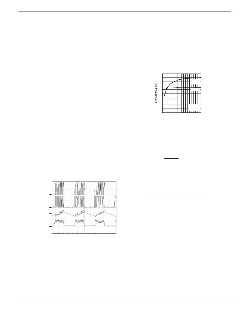
�Figure� 4� shows� the� improvement� in� ef?ciency� that� SKIP� mode�
�makes� when� at� lower� output� currents.�
�MIC2185� PWM� vs.�
�Skip� Mode� Efficiency�
�100�
�80�
�60� SKIP�
�40�
�20�
�V� OUT� =5V�
�0�
�OUTPUT� CURRENT� (A)�
�Figure� 4.�
�The� maximum� peak� inductor� current� depends� on� the� skip�
�current� limit� threshold� and� the� value� of� the� current� sense�
�resistor,� R� SENSE� .� For� a� typical� 50mV� current� limit� threshold�
�in� skip� mode,� the� peak� inductor� current� is:�
�50mV�
�R� SENSE�
�The� maximum� output� current� in� skip� mode� depends� on� the�
�input� conditions,� output� conditions� and� circuit� component�
�values.� Assuming� a� discontinuous� mode� where� the� inductor�
�current� starts� from� zero� at� each� cycle,� the� maximum� output�
�current� is� calculated� below:�
�2.5� � 10� ?� 3� � L� � fs�
�2� ×� R� SENSE� 2� ×� (� V� O� ?� (� η� ×� V� IN� )� )�
�where:� I� O(max)� is� the� maximum� output� current�
�V� O� is� the� output� voltage�
�V� IN� is� the� input� voltage�
�L� is� the� value� of� the� boost� inductor�
�f� S� is� the� switching� frequency�
�η� is� the� ef?ciency� of� the� boost� converter�
�R� SENSE� is� the� value� of� the� current� sense� resistor�
�2.5·10� -3� is� a� constant� based� on� the� skip� mode�
�current� threshold� (50mV)� 2�
�October� 2005�
�9�
�MIC2185�
�相关PDF资料 |
PDF描述 |
|---|---|
| GCM30DTBT | CONN EDGECARD 60POS R/A .156 SLD |
| EMC08DRTN-S734 | CONN EDGECARD 16POS DIP .100 SLD |
| UPM2A391MHD | CAP ALUM 390UF 100V 20% RADIAL |
| ISL88706IP829Z | IC SUPERVISOR MPU 2.92V 8-PDIP |
| MIC2186BM TR | IC REG CTRLR BST FLYBK CM 16SOIC |
相关代理商/技术参数 |
参数描述 |
|---|---|
| MIC2185YM | 功能描述:DC/DC 开关控制器 SO-16 Low Vin Synchronous Buck PWM Control IC (Lead Free) RoHS:否 制造商:Texas Instruments 输入电压:6 V to 100 V 开关频率: 输出电压:1.215 V to 80 V 输出电流:3.5 A 输出端数量:1 最大工作温度:+ 125 C 安装风格: 封装 / 箱体:CPAK |
| MIC2185YM TR | 功能描述:DC/DC 开关控制器 SO-16 Low Vin Synchronous Buck PWM Control IC (Lead Free) RoHS:否 制造商:Texas Instruments 输入电压:6 V to 100 V 开关频率: 输出电压:1.215 V to 80 V 输出电流:3.5 A 输出端数量:1 最大工作温度:+ 125 C 安装风格: 封装 / 箱体:CPAK |
| MIC2185YQS | 功能描述:DC/DC 开关控制器 SO-16 Low Vin Synchronous Buck PWM Control IC (Lead Free) RoHS:否 制造商:Texas Instruments 输入电压:6 V to 100 V 开关频率: 输出电压:1.215 V to 80 V 输出电流:3.5 A 输出端数量:1 最大工作温度:+ 125 C 安装风格: 封装 / 箱体:CPAK |
| MIC2185YQS TR | 功能描述:DC/DC 开关控制器 SO-16 Low Vin Synchronous Buck PWM Control IC (Lead Free) RoHS:否 制造商:Texas Instruments 输入电压:6 V to 100 V 开关频率: 输出电压:1.215 V to 80 V 输出电流:3.5 A 输出端数量:1 最大工作温度:+ 125 C 安装风格: 封装 / 箱体:CPAK |
| MIC2186 | 制造商:MICREL 制造商全称:Micrel Semiconductor 功能描述:Low Voltage PWM Control IC |
发布紧急采购,3分钟左右您将得到回复。