- 您现在的位置:买卖IC网 > PDF目录15113 > MIC2186BQS (Micrel Inc)IC REG CTRLR BST FLYBK CM 16QSOP PDF资料下载
参数资料
| 型号: | MIC2186BQS |
| 厂商: | Micrel Inc |
| 文件页数: | 14/15页 |
| 文件大小: | 0K |
| 描述: | IC REG CTRLR BST FLYBK CM 16QSOP |
| 标准包装: | 98 |
| PWM 型: | 电流模式 |
| 输出数: | 1 |
| 频率 - 最大: | 440kHz |
| 占空比: | 85% |
| 电源电压: | 2.9 V ~ 14 V |
| 降压: | 无 |
| 升压: | 是 |
| 回扫: | 是 |
| 反相: | 无 |
| 倍增器: | 无 |
| 除法器: | 无 |
| Cuk: | 无 |
| 隔离: | 无 |
| 工作温度: | -40°C ~ 125°C |
| 封装/外壳: | 16-SSOP(0.154",3.90mm 宽) |
| 包装: | 管件 |
�� �
�
�MIC2186�
�MIC2186�
�Micrel,� Inc.�
�maximum� output� current.�
�*� Allow� the� MIC2186� to� run� in� skip� mode� at� lower�
�Voltage�
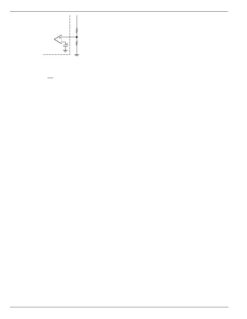
�Amplifier�
�Pin�
�R1�
�currents.� If� running� in� PWM� mode,� set� the�
�MIC2186� to� switch� at� a� lower� frequency.�
�*� se� a� ferrite� material� for� the� inductor� core,� which�
�V� REF�
�1.245V�
�6�
�R2�
�has� less� core� loss� than� an� MPP� or� iron� power�
�core.�
�The� significant� contributors� to� power� loss� at� higher� output�
�V� O� =� V� REF� � 1� +�
�Figure 11.�
�The� output� voltage� is� determined� by� the� equation� below.�
�R1�
�R2�
�Where:� Vref� for� the� MIC2186� is� nominally� 1.245V.� Lower�
�values� of� resistance� are� preferred� to� prevent� noise� from�
�apprearing� on� the� Vfb� pin.� A� typically� recommended� value� for�
�R1� is� 10K.�
�Decoupling� Capacitor� Selection�
�The� 1uf� decoupling� capacitor� is� used� to� stabilize� the� internal�
�regulator� and� minimize� noise� on� the� Vdd� pin.� Placement� of�
�this� capacitor� is� critical� to� the� proper� operation� of� the� MIC2186.�
�It� must� be� next� to� the� Vdd� and� signal� ground� pins� and� routed�
�with� wide� etch.� The� capacitor� should� be� a� good� quality�
�ceramic.� Incorrect� placement� of� the� Vdd� decoupling� capaci-�
�tor� will� cause� jitter� and/or� oscillations� in� the� switching� wave-�
�form� as� well� as� variations� in� the� overcurrent� limit.�
�A� minimum� 0.1uf� ceramic� capacitor� is� required� to� decouple�
�the� Vin.� The� capacitor� should� be� placed� near� the� IC� and�
�connected� directly� between� pins� 10� (Vcc)� and� 5� (SGND).� A�
�0.1uf� capacitor� is� required� to� decouple� Vref.� It� should� be�
�located� near� the� Vref� pin.�
�Efficiency� calculation� and� considerations�
�Efficiency� is� the� ratio� of� output� power� to� input� power.� The�
�difference� is� dissipated� as� heat� in� the� boost� converter.� The�
�significant� contributors� at� light� output� loads� are:�
�*� The� VinA� pin� supply� current.�
�*� The� VinP� pin� supply� current� which� includes� the�
�current� required� to� switch� the� external�
�MOSFETs�
�*� Core� losses� in� the� inductor�
�To� maximize� efficiency� at� light� loads:�
�*� Use� a� low� gate� charge� MOSFET� or� use� the�
�smallest� MOSFET,� which� is� still� adequate� for� the�
�loads� are� (in� approximate� order� of� magnitude):�
�*� Resistive� on-time� losses� in� the� MOSFET�
�*� Switching� transition� losses� in� the� MOSFET�
�*� Inductor� resistive� losses�
�*� Current� sense� resistor� losses�
�*� Output� capacitor� resistive� losses� (due� to� the�
�capacitor’s� ESR)�
�To� minimize� power� loss� under� heavy� loads:�
�*� Use� Logic� level,� low� on� resistance� MOSFETs.�
�Multiplying� the� gate� charge� by� the� on� resistance�
�gives� a� figure� of� merit,� providing� a� good� balance�
�between� switching� and� resistive� power� dissipa-�
�tion.�
�*� Slow� transition� times� and� oscillations� on� the�
�voltage� and� current� waveforms� dissipate� more�
�power� during� the� turn-on� and� turn-off� of� the� low�
�side� MOSFET.� A� clean� layout� will� minimize�
�parasitic� inductance� and� capacitance� in� the� gate�
�drive� and� high� current� paths.� This� will� allow� the�
�fastest� transition� times� and� waveforms� without�
�oscillations.� Low� gate� charge� MOSFETs� will�
�switch� faster� than� those� with� higher� gate� charge�
�specifications.�
�*� For� the� same� size� inductor,� a� lower� value� will�
�have� fewer� turns� and� therefore,� lower� winding�
�resistance.� However,� using� too� small� of� a� value�
�will� increase� the� inductor� current� and� therefore�
�require� more� output� capacitors� to� filter� the� output�
�ripple.�
�*� Lowering� the� current� sense� resistor� value� will�
�decrease� the� power� dissipated� in� the� resistor.�
�However,� it� will� also� increase� the� overcurrent�
�limit� and� may� require� larger� MOSFETs� and�
�inductor� components� to� handle� the� higher�
�currents.�
�*� Use� low� ESR� output� capacitors� to� minimize� the�
�power� dissipated� in� the� capacitor’s� ESR.�
�M9999-042205�
�14�
�April� 2005�
�相关PDF资料 |
PDF描述 |
|---|---|
| ISL88706IB826Z | IC SUPERVISOR 2.63V 8-SOIC |
| ESC10DRTN-S734 | CONN EDGECARD 20POS DIP .100 SLD |
| VE-24V-EW-F2 | CONVERTER MOD DC/DC 5.8V 100W |
| ISL88705IB846Z | IC SUPERVISOR 4.64V 8-SOIC |
| ISL88706IP844Z | IC SUPERVISOR MPU 4.38V 8-PDIP |
相关代理商/技术参数 |
参数描述 |
|---|---|
| MIC2186BQS TR | 功能描述:IC REG CTRLR BST FLYBK CM 16QSOP RoHS:否 类别:集成电路 (IC) >> PMIC - 稳压器 - DC DC 切换控制器 系列:- 标准包装:4,000 系列:- PWM 型:电压模式 输出数:1 频率 - 最大:1.5MHz 占空比:66.7% 电源电压:4.75 V ~ 5.25 V 降压:是 升压:无 回扫:无 反相:无 倍增器:无 除法器:无 Cuk:无 隔离:无 工作温度:-40°C ~ 85°C 封装/外壳:40-VFQFN 裸露焊盘 包装:带卷 (TR) |
| MIC2186YM | 功能描述:DC/DC 开关控制器 SO-16 Low Vin Synchronous Buck PWM Control IC (Lead Free) RoHS:否 制造商:Texas Instruments 输入电压:6 V to 100 V 开关频率: 输出电压:1.215 V to 80 V 输出电流:3.5 A 输出端数量:1 最大工作温度:+ 125 C 安装风格: 封装 / 箱体:CPAK |
| MIC2186YM TR | 功能描述:DC/DC 开关控制器 SO-16 Low Vin Synchronous Buck PWM Control IC (Lead Free) RoHS:否 制造商:Texas Instruments 输入电压:6 V to 100 V 开关频率: 输出电压:1.215 V to 80 V 输出电流:3.5 A 输出端数量:1 最大工作温度:+ 125 C 安装风格: 封装 / 箱体:CPAK |
| MIC2186YQS | 功能描述:DC/DC 开关控制器 SO-16 Low Vin Synchronous Buck PWM Control IC (Lead Free) RoHS:否 制造商:Texas Instruments 输入电压:6 V to 100 V 开关频率: 输出电压:1.215 V to 80 V 输出电流:3.5 A 输出端数量:1 最大工作温度:+ 125 C 安装风格: 封装 / 箱体:CPAK |
| MIC2186YQS TR | 功能描述:DC/DC 开关控制器 SO-16 Low Vin Synchronous Buck PWM Control IC (Lead Free) RoHS:否 制造商:Texas Instruments 输入电压:6 V to 100 V 开关频率: 输出电压:1.215 V to 80 V 输出电流:3.5 A 输出端数量:1 最大工作温度:+ 125 C 安装风格: 封装 / 箱体:CPAK |
发布紧急采购,3分钟左右您将得到回复。