- 您现在的位置:买卖IC网 > PDF目录15113 > MIC2194BM (Micrel Inc)IC REG CTRLR BST PWM CM 8-SOIC PDF资料下载
参数资料
| 型号: | MIC2194BM |
| 厂商: | Micrel Inc |
| 文件页数: | 8/10页 |
| 文件大小: | 0K |
| 描述: | IC REG CTRLR BST PWM CM 8-SOIC |
| 标准包装: | 95 |
| PWM 型: | 电流模式 |
| 输出数: | 1 |
| 频率 - 最大: | 440kHz |
| 占空比: | 100% |
| 电源电压: | 2.9 V ~ 14 V |
| 降压: | 是 |
| 升压: | 是 |
| 回扫: | 无 |
| 反相: | 无 |
| 倍增器: | 无 |
| 除法器: | 无 |
| Cuk: | 无 |
| 隔离: | 无 |
| 工作温度: | -40°C ~ 125°C |
| 封装/外壳: | 8-SOIC(0.154",3.90mm 宽) |
| 包装: | 管件 |
�� �
�
�MIC2194�
�MIC2194�
�MOSFET� Selection�
�Micrel�
�V� IN�
�R1�
�1.5V�
�Typical�
�Bias�
�Circuitry�
�The� P-channel� MOSFET� must� have� a� V� GS� threshold� voltage�
�equal� to� or� lower� than� the� input� voltage� when� used� in� a� buck�
�converter� topology.� There� is� a� limit� to� the� maximum� gate�
�charge� the� MIC2194� will� drive.� MOSFETs� with� high� gate�
�charge� will� have� slower� turn-on� and� turn-off� times.� Slower�
�R2�
�EN/UVLO�
�(3)�
�140mV�
�Hysteresis�
�(typical)�
�transition� times� will� cause� higher� power� dissipation� in� the�
�MOSFET� due� to� higher� switching� transition� losses.�
�The� MOSFET� gate� charge� is� also� limited� by� power� dissipation�
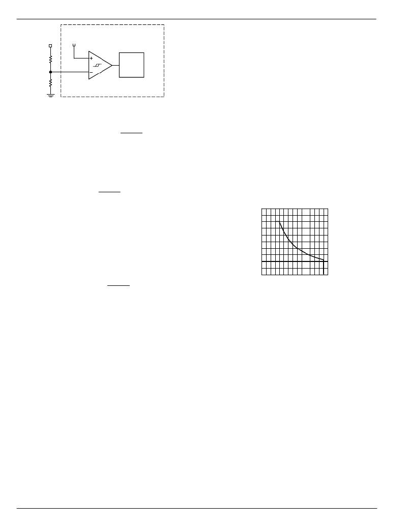
�V� INPUT� _� ENABLE� =� V� THRESHOLD� �
�Figure� 3.� UVLO� Circuitry�
�The� line� voltage� turn� on� trip� point� is:�
�R� 2�
�R� 1� +� R� 2�
�where:�
�V� THRESHOLD� is� the� voltage� level� of� the� internal�
�comparator� reference,� typically� 1.5V.�
�The� input� voltage� hysteresis� is� equal� to:�
�in� the� MIC2194.� The� power� dissipated� by� the� gate� drive�
�circuitry� is� calculated� below:�
�P� GATE_DRIVE� =� Q� GATE� � V� IN� � f� S�
�where:� Q� GATE� is� the� total� gate� charge� of� both� the� N-� and� P-�
�channel� MOSFETs.�
�f� S� is� the� switching� frequency�
�V� IN� is� the� gate� drive� voltage�
�The� graph� in� Figure� 4� shows� the� total� gate� charge� that� can� be�
�driven� by� the� MIC2194� over� the� input� voltage� range,� for�
�V� INPUT� _� HYST� =� V� HYST� �
�R1� +� R 2�
�R� 2�
�different� values� of� switching� frequency.�
�Max� Gate� Charge�
�(V� THRESHOLD� –� V� HYST� )� ×�
�where:�
�V� HYST� is� the� internal� comparator� hysteresis� level,�
�typically� 140mV.�
�V� INPUT_HYST� is� the� hysteresis� at� the� input� voltage�
�The� MIC2194� will� be� disabled� when� the� input� voltage� drops�
�back� down� to:�
�V� INPUT_OFF� =�
�V� INPUT_ENABLE� –� V� INPUT_HYST� =�
�R� 2�
�R� 1� +� R� 2�
�Either� of� 2� UVLO� conditions� will� pull� the� soft� start� capacitor�
�low:�
�?� When� the� V� DD� voltage� drops� below� its�
�undervoltage� lockout� level.�
�?� When� the� enable� pin� drops� below� the� its� enable�
�threshold�
�The� internal� bias� circuit� generates� an� internal� 1.245V� band-�
�gap� reference� voltage� for� the� voltage� error� amplifier� and� a� 3V�
�VDD� voltage� for� the� internal� control� circuitry.� The� VDD� pin�
�must� be� decoupled� with� a� 1� μ� F� ceramic� capacitor.� The� capaci-�
�tor� must� be� placed� close� to� the� VDD� pin.� The� other� end� of� the�
�capacitor� must� be� connected� directly� to� the� ground� plane.�
�MOSFET� Gate� Drive�
�The� MIC2194� is� designed� to� drive� a� high-side� P-channel�
�MOSFET.� The� source� pin� of� the� P-channel� MOSFET� is�
�connected� to� the� input� of� the� power� supply.� It� is� turned� on�
�when� OUTP� pulls� the� gate� of� the� MOSFET� low.� The� advan-�
�tage� of� using� a� P-channel� MOSFET� is� that� it� does� not� require�
�a� bootstrap� circuit� to� boost� the� gate� voltage� higher� than� the�
�input,� as� would� be� required� for� an� N-channel� MOSFET.� The�
�VIN� pin� (pin� 8)� supplies� the� drive� voltage� to� the� gate� drive� pin,�
�OUTP.�
�250�
�200�
�150�
�100�
�50�
�0�
�0� 5� 10� 15�
�INPUT� VOLTAGE� (V)�
�Figure� 4.� MIC2194� V� IN� vs� Max.� Gate� Charge�
�Oscillator�
�The� internal� oscillator� is� free� running� and� requires� no� external�
�components.� The� maximum� duty� cycle� for� both� frequencies�
�is� 100%.� This� is� another� advantage� of� using� a� P-channel�
�MOSFET� for� the� high-side� drive;� it� can� be� continuously� turned�
�on.�
�A� frequency� foldback� mode� is� enabled� if� the� voltage� on� the�
�feedback� pin� (pin� 2)� is� less� than� 0.3V.� In� frequency� foldback,�
�the� oscillator� frequency� is� reduced� by� approximately� a� factor�
�of� 4.� Frequency� foldback� is� used� to� limit� the� energy� delivered�
�to� the� output� during� a� short� circuit� fault� condition.�
�Voltage� Setting� Components�
�The� MIC2194� requires� two� resistors� to� set� the� output� voltage�
�as� shown� in� Figure� 5.�
�MIC2194�
�8�
�April� 2005�
�相关PDF资料 |
PDF描述 |
|---|---|
| RCC13DRTI-S734 | CONN EDGECARD 26POS .100 EXTEND |
| UCD2A221MNQ1MS | CAP ALUM 220UF 100V 20% SMD |
| ISL88708IB831Z | IC SUPERVISOR 3.09V 8-SOIC |
| UVP0J682MHD | CAP ALUM 6800UF 6.3V 20% RADIAL |
| RSM11DRYF | CONN EDGECARD 22POS DIP .156 SLD |
相关代理商/技术参数 |
参数描述 |
|---|---|
| MIC2194BM TR | 功能描述:IC REG CTRLR BST PWM CM 8-SOIC RoHS:否 类别:集成电路 (IC) >> PMIC - 稳压器 - DC DC 切换控制器 系列:- 标准包装:4,000 系列:- PWM 型:电压模式 输出数:1 频率 - 最大:1.5MHz 占空比:66.7% 电源电压:4.75 V ~ 5.25 V 降压:是 升压:无 回扫:无 反相:无 倍增器:无 除法器:无 Cuk:无 隔离:无 工作温度:-40°C ~ 85°C 封装/外壳:40-VFQFN 裸露焊盘 包装:带卷 (TR) |
| MIC2194YM | 功能描述:DC/DC 开关控制器 SO-8 3V Buck Contoller (Lead Free) RoHS:否 制造商:Texas Instruments 输入电压:6 V to 100 V 开关频率: 输出电压:1.215 V to 80 V 输出电流:3.5 A 输出端数量:1 最大工作温度:+ 125 C 安装风格: 封装 / 箱体:CPAK |
| MIC2194YM TR | 功能描述:DC/DC 开关控制器 SO-8 3V Buck Contoller (Lead Free) RoHS:否 制造商:Texas Instruments 输入电压:6 V to 100 V 开关频率: 输出电压:1.215 V to 80 V 输出电流:3.5 A 输出端数量:1 最大工作温度:+ 125 C 安装风格: 封装 / 箱体:CPAK |
| MIC2196 | 制造商:MICREL 制造商全称:Micrel Semiconductor 功能描述:400kHz SO-8 Boost Control IC |
| MIC2196_08 | 制造商:MICREL 制造商全称:Micrel Semiconductor 功能描述:400kHz SO-8 Boost Control IC |
发布紧急采购,3分钟左右您将得到回复。