- 您现在的位置:买卖IC网 > PDF目录22125 > MIC2585-1KYTS (Micrel Inc)IC CTRLR HOT SWAP DUAL 24-TSSOP PDF资料下载
参数资料
| 型号: | MIC2585-1KYTS |
| 厂商: | Micrel Inc |
| 文件页数: | 22/28页 |
| 文件大小: | 273K |
| 描述: | IC CTRLR HOT SWAP DUAL 24-TSSOP |
| 标准包装: | 62 |
| 类型: | 热交换控制器 |
| 应用: | 通用 |
| 内部开关: | 无 |
| 电源电压: | 1 V ~ 13.2 V |
| 工作温度: | -40°C ~ 85°C |
| 安装类型: | 表面贴装 |
| 封装/外壳: | 24-TSSOP(0.173",4.40mm 宽) |
| 供应商设备封装: | 24-TSSOP |
| 包装: | 管件 |
第1页第2页第3页第4页第5页第6页第7页第8页第9页第10页第11页第12页第13页第14页第15页第16页第17页第18页第19页第20页第21页当前第22页第23页第24页第25页第26页第27页第28页
MIC2584/2585
Micrel
MIC2584/2585
22
March 2005
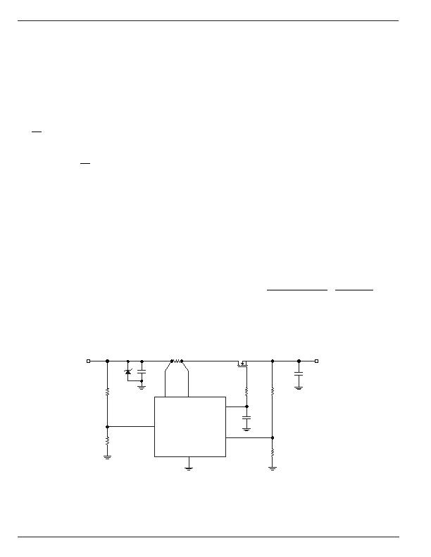
Higher UVLO Setting
Once a PCB is inserted into a backplane (power supply), the
internal UVLO circuit of the MIC2584/85 holds the GATE
output charge pump off until VCC1 exceeds 2.165V and
VCC2 exceeds 0.8V. If VCC1 falls below 1.935V or VCC2
falls below 0.77V, the UVLO circuit pulls the GATE output to
ground and clears the overvoltage and/or current limit faults.
For a higher UVLO threshold, the circuit in Figure 10 can be
used to delay the output MOSFET from switching on until the
desired input voltage is achieved. The circuit allows the
charge pumps to remain off until V
IN1
exceeds
1
R1
R2
1.235V
+
?/DIV>
?/DIV>
?/DIV>
?/DIV>
?/DIV>
?/DIV>
?/DIV>
provided that VCC2 has exceeded its
threshold. Both GATE drive outputs will be shut down when
V
IN1
falls below
1
R1
R2
1.21V
+
?/DIV>
?/DIV>
?/DIV>
?/DIV>
?/DIV>
?/DIV>
?/DIV>
. In the example circuit , the
rising UVLO threshold is set at approximately 9.0V and the
falling UVLO threshold is established as 8.9V. The circuit
consists of an external resistor divider at the ON pin that
keeps both GATE output charge pumps off until the voltage
at the ON pin exceeds its threshold (V
ON
) and after the start-
up timer elapses.
Hot Swap Power Control for DSPs
In designing power supplies for dual supply logic devices,
such as a DSP, consideration should be given to the system
timing requirements of the core and I/O voltages for power-
up and power-down operations. When power is provided to
the core and I/O circuit blocks in an unpredictable manner,
the effects can be detrimental to the life cycle of the DSP or
logic device by allowing unexpected current to flow in the core
and I/O isolation structures. Additionally, bus contention is
one of the critical system-level issues supporting the need for
power supply sequencing. Since the core supplies logic
control for the bus, powering up the I/O before the core may
result in both the DSP and an attached peripheral device
being simultaneously configured as outputs. In this case, the
output drivers of each device contend for control over sending
data along the bus which may cause excessive current to flow
in one of the paths (I
1
or I
2
) shown in the bidirectional port of
Figure 11. Upon powering down the system, the core voltage
supply should turn off after the I/O as the bus control signal(s)
may enter an indeterminate state if the core is powered down
first. Thus, for power sequencing of a dual supply voltage
DSP implementing the MIC2585 (if V
CORE
e V
I/O
), a circuit
similar to Figure 8 is recommended with the core voltage
supplied through Channel 1 and the I/O voltage supplied
through Channel 2. For systems with V
CORE
< V
I/O
, the
MIC2585-2 option with the I/O voltage through Channel 1 and
core through Channel 2 is used to implement the first on-last
off application.
Sense Resistor Selection
The MIC2584 and MIC2585 use a low-value sense resistor to
measure the current flowing through the MOSFET switch
(and therefore the load). This sense resistor is nominally set
at 50mV/I
LOAD(CONT)
. To accommodate worst-case toler-
ances for both the sense resistor (allow ?% over time and
temperature for a resistor with ?% initial tolerance) and still
supply the maximum required steady-state load current, a
slightly more detailed calculation must be used.
The current limit threshold voltage (i.e., the
trip point
) for the
MIC2584/85 may be as low as 42.5mV, which would equate
to a sense resistor value of 42.5mV/I
LOAD(CONT)
. Carrying the
numbers through for the case where the value of the sense
resistor is 3% high yields:
R
42.5mV
1.03 I
41.3mV
I
SENSE(MAX)
LOAD(CONT)
LOAD(CONT)
=
( )
(
)
=
(11)
Once the value of R
SENSE
has been chosen in this manner,
it is good practice to check the maximum I
LOAD(CONT)
which
the circuit may let through in the case of tolerance build-up in
SENSE1
VCC1
ON
FB1
GATE1
GND
Undervoltage Lockout Threshold (rising) = 9.0V
Undervoltage Lockout Threshold (falling) = 8.9V
Undervoltage (Output) = 11.4V
Channel 2 and additional pins omitted for clarity.
Q1
IRF7822
(SO-8)
R3
10&
R5
16.2k&
1%
R1
154k&
1%
R2
24.3k&
1%
MIC2584
C1
1礔
D1
(18V)
C2
0.01礔
C
LOAD1
1000礔
R4
133k&
1%
V
OUT1
12V@4A
V
IN1
12V
9
16
15
12
6
14
R
SENSE1
0.010&
5%
1
2
3
4
Figure 10. Higher UVLO Setting
相关PDF资料 |
PDF描述 |
|---|---|
| M4A5-32/32-12JNI | IC CPLD 32MACRO 44PLCC |
| TAP105M020BRS | CAP TANT 1UF 20V 20% RADIAL |
| MIC2585-2JYTS | IC CTRLR HOT SWAP DUAL 24-TSSOP |
| GRM219R61E225KA12D | CAP CER 2.2UF 25V 10% X5R 0805 |
| M4A5-32/32-10JNC | IC CPLD 32MACRO 44PLCC |
相关代理商/技术参数 |
参数描述 |
|---|---|
| MIC2585-1KYTS TR | 功能描述:热插拔功率分布 Dual Channel Hot-Swap Controller - 100mV Threshold (Lead Free) RoHS:否 制造商:Texas Instruments 产品:Controllers & Switches 电流限制: 电源电压-最大:7 V 电源电压-最小:- 0.3 V 工作温度范围: 功率耗散: 安装风格:SMD/SMT 封装 / 箱体:MSOP-8 封装:Tube |
| MIC2585-1LBTS | 功能描述:IC CTRLR HOT SWAP DUAL 24-TSSOP RoHS:否 类别:集成电路 (IC) >> PMIC - 热交换 系列:- 产品培训模块:Obsolescence Mitigation Program 标准包装:100 系列:- 类型:热插拔开关 应用:通用 内部开关:是 电流限制:可调 电源电压:9 V ~ 13.2 V 工作温度:-40°C ~ 150°C 安装类型:表面贴装 封装/外壳:10-WFDFN 裸露焊盘 供应商设备封装:10-TDFN-EP(3x3) 包装:管件 |
| MIC2585-1LBTS TR | 功能描述:IC CTRLR HOT SWAP DUAL 24-TSSOP RoHS:否 类别:集成电路 (IC) >> PMIC - 热交换 系列:- 产品培训模块:Obsolescence Mitigation Program 标准包装:100 系列:- 类型:热插拔开关 应用:通用 内部开关:是 电流限制:可调 电源电压:9 V ~ 13.2 V 工作温度:-40°C ~ 150°C 安装类型:表面贴装 封装/外壳:10-WFDFN 裸露焊盘 供应商设备封装:10-TDFN-EP(3x3) 包装:管件 |
| MIC2585-1LYTS | 功能描述:热插拔功率分布 Dual Channel Hot-Swap Controller - 100mV Threshold (Lead Free) RoHS:否 制造商:Texas Instruments 产品:Controllers & Switches 电流限制: 电源电压-最大:7 V 电源电压-最小:- 0.3 V 工作温度范围: 功率耗散: 安装风格:SMD/SMT 封装 / 箱体:MSOP-8 封装:Tube |
| MIC2585-1LYTS TR | 功能描述:热插拔功率分布 Dual Channel Hot-Swap Controller - 100mV Threshold (Lead Free) RoHS:否 制造商:Texas Instruments 产品:Controllers & Switches 电流限制: 电源电压-最大:7 V 电源电压-最小:- 0.3 V 工作温度范围: 功率耗散: 安装风格:SMD/SMT 封装 / 箱体:MSOP-8 封装:Tube |
发布紧急采购,3分钟左右您将得到回复。