参数资料
| 型号: | MIC26600YJL TR |
| 厂商: | Micrel Inc |
| 文件页数: | 14/28页 |
| 文件大小: | 0K |
| 描述: | IC REG BUCK SYNC ADJ 7A 28-MLF |
| 产品培训模块: | SuperSwitcherII™ - Step Down DC-DC Regulator Family |
| 标准包装: | 1 |
| 系列: | Hyper Speed Control™,SuperSwitcher II™ |
| 类型: | 降压(降压) |
| 输出类型: | 可调式 |
| 输出数: | 1 |
| 输出电压: | 可调至 0.8V |
| 输入电压: | 4.5 V ~ 26 V |
| PWM 型: | 混合物 |
| 频率 - 开关: | 300kHz |
| 电流 - 输出: | 7A |
| 同步整流器: | 是 |
| 工作温度: | -40°C ~ 125°C |
| 安装类型: | 表面贴装 |
| 封装/外壳: | 28-VQFN 裸露焊盘,28-MLF? |
| 包装: | 标准包装 |
| 供应商设备封装: | 28-MLF?(5x6) |
| 其它名称: | 576-3716-6 |
第1页第2页第3页第4页第5页第6页第7页第8页第9页第10页第11页第12页第13页当前第14页第15页第16页第17页第18页第19页第20页第21页第22页第23页第24页第25页第26页第27页第28页
�� �
�
�Micrel,� Inc.�
�Functional� Description�
�The� MIC26600� is� an� adaptive� ON-time� synchronous�
�step-down� DC-DC� regulator.� It� is� designed� to� operate�
�over� a� wide� input� voltage� range� from,� 4.5V� to� 26V,� and�
�provides� a� regulated� output� voltage� at� up� to� 7A� of� output�
�current.� A� digitally� modified� adaptive� ON-time� control�
�scheme� is� employed� in� to� obtain� a� constant� switching�
�frequency� and� to� simplify� the� control� compensation.�
�Over-current� protection� is� implemented� without� the� use�
�of� an� external� sense� resistor.� The� device� includes� an�
�internal� soft-start� function� which� reduces� the� power�
�supply� input� surge� current� at� start-up� by� controlling� the�
�output� voltage� rise� time.�
�Theory� of� Operation�
�Figure� 1� illustrates� the� block� diagram� for� the� control� loop�
�of� the� MIC26600.� The� output� voltage� is� sensed� by� the�
�MIC26600� feedback� pin� FB� via� the� voltage� divider� R1�
�and� R2,� and� compared� to� a� 0.8V� reference� voltage� V� REF�
�at� the� error� comparator� through� a� low� gain�
�transconductance� (g� m� )� amplifier.� If� the� feedback� voltage�
�decreases� and� the� output� of� the� g� m� amplifier� is� below�
�0.8V,� then� the� error� comparator� will� trigger� the� control�
�logic� and� generate� an� ON-time� period.� The� ON-time�
�period� length� is� predetermined� by� the� “FIXED� t� ON�
�ESTIMATION”� circuitry:�
�MIC26600�
�It� is� not� recommended� to� use� MIC26600� with� a� OFF-time�
�close� to� t� OFF(min)� during� steady-state� operation.� Also,� as�
�V� OUT� increases,� the� internal� ripple� injection� will� increase�
�and� reduce� the� line� regulation� performance.� Therefore,�
�the� maximum� output� voltage� of� the� MIC26600� should� be�
�limited� to� 5.5V.� Please� refer� to� “Setting� Output� Voltage”�
�subsection� in� “Application� Information”� for� more� details.�
�The� actual� ON-time� and� resulting� switching� frequency�
�will� vary� with� the� part-to-part� variation� in� the� rise� and� fall�
�times� of� the� internal� MOSFETs,� the� output� load� current,�
�and� variations� in� the� V� DD� voltage.� Also,� the� minimum� t� ON�
�results� in� a� lower� switching� frequency� in� high� V� IN� to� V� OUT�
�applications,� such� as� 26V� to� 1.0V.� The� minimum� t� ON�
�measured� on� the� MIC26600� evaluation� board� is� about�
�184ns.� During� load� transients,� the� switching� frequency� is�
�changed� due� to� the� varying� OFF-time.�
�To� illustrate� the� control� loop� operation,� will� be� analyzed�
�both� the� steady-state� and� load� transient� scenarios.� For�
�easy� analysis,� the� gain� of� the� g� m� amplifier� is� assumed� to�
�be� 1.� With� this� assumption,� the� inverting� input� of� the�
�error� comparator� is� the� same� as� the� feedback� voltage.�
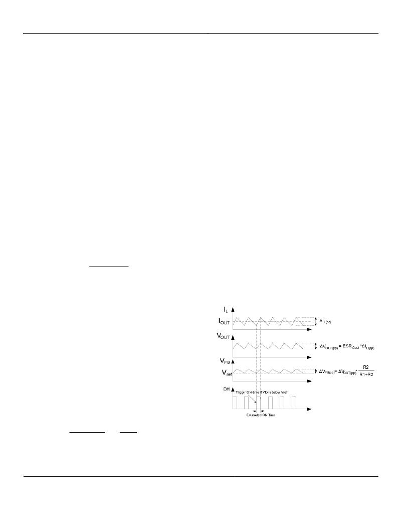
�Figure� 2� shows� the� MIC26600� control� loop� timing� during�
�steady-state� operation.� During� steady-state,� the� g� m�
�amplifier� senses� the� feedback� voltage� ripple,� which� is�
�proportional� to� the� output� voltage� ripple� and� the� inductor�
�current� ripple,� to� trigger� the� ON-time� period.� The� ON-�
�t� ON(estimat� ed)� =�
�V� OUT�
�V� IN� � 300kHz�
�(1)�
�time� is� predetermined� by� the� t� ON� estimator.� The�
�termination� of� the� OFF-time� is� controlled� by� the� feedback�
�voltage.� At� the� valley� of� the� feedback� voltage� ripple,�
�which� occurs� when� V� FB� falls� below� V� REF� ,� the� OFF� period�
�ends� and� the� next� ON-time� period� is� triggered� through�
�where� V� OUT� is� the� output� voltage� and� V� IN� is� the� power�
�stage� input� voltage.�
�At� the� end� of� the� ON-time� period,� the� internal� high-side�
�driver� turns� off� the� high-side� MOSFET� and� the� low-side�
�driver� turns� on� the� low-side� MOSFET.� The� OFF-time�
�period� length� depends� upon� the� feedback� voltage� in�
�most� cases.� When� the� feedback� voltage� decreases� and�
�the� output� of� the� g� m� amplifier� is� below� 0.8V,� the� ON-time�
�period� is� triggered� and� the� OFF-time� period� ends.� If� the�
�OFF-time� period� determined� by� the� feedback� voltage� is�
�less� than� the� minimum� OFF-time� t� OFF(min)� ,� which� is� about�
�360ns,� the� MIC26600� control� logic� will� apply� the� t� OFF(min)�
�instead.� t� OFF(min)� is� required� to� maintain� enough� energy� in�
�the� boost� capacitor� (C� BST� )� to� drive� the� high-side�
�MOSFET.� The� maximum� duty� cycle� is� obtained� from� the�
�360ns� t� OFF(min)� :�
�the� control� logic� circuitry.�
�D� max� =�
�t� S� ?� t� OFF(min)�
�t� S�
�=� 1� ?�
�360ns�
�t� S�
�(2)�
�Figure� 2.� MIC26600� Control� Loop� Timing�
�where� t� S� =� 1/300kHz� =� 3.33� μ� s.�
�July� 2011�
�14�
�M9999-070111-C�
�相关PDF资料 |
PDF描述 |
|---|---|
| MIC26601YJL TR | IC REG BUCK SYNC ADJ 6A 28MLF |
| MIC26603YJL TR | IC REG BUCK SYNC ADJ 6A 28MLF |
| MIC26901YJL TR | IC REG BUCK SYNC ADJ 9A 28MLF |
| MIC26903YJL TR | IC REG BUCK SYNC ADJ 9A 28MLF |
| MIC26950YJL TR | IC REG BUCK SYNC ADJ 12A 28-MLF |
相关代理商/技术参数 |
参数描述 |
|---|---|
| MIC26601YJL EV | 功能描述:电源管理IC开发工具 28V/6A DC-DC Buck Regulator w/ HSC - Evaluation Board RoHS:否 制造商:Maxim Integrated 产品:Evaluation Kits 类型:Battery Management 工具用于评估:MAX17710GB 输入电压: 输出电压:1.8 V |
| MIC26601YJL TR | 功能描述:直流/直流开关调节器 28V/6A DC-DC Buck Regulator w/ HSC RoHS:否 制造商:International Rectifier 最大输入电压:21 V 开关频率:1.5 MHz 输出电压:0.5 V to 0.86 V 输出电流:4 A 输出端数量: 最大工作温度: 安装风格:SMD/SMT 封装 / 箱体:PQFN 4 x 5 |
| MIC26601YJLEV | 制造商:Micrel Inc 功能描述:Evaluation Board for MIC26601YJL |
| MIC26601YJL-EV | 功能描述:MIC26601 Hyper Speed Control?, SuperSwitcher II? DC/DC, Step Down 1, Non-Isolated Outputs Evaluation Board 制造商:microchip technology 系列:Hyper Speed Control?,SuperSwitcher II? 零件状态:无货 主要用途:DC/DC,步降 输出和类型:1,非隔离 功率 - 输出:- 电压 - 输出:5V 电流 - 输出:6A 电压 - 输入:5.5 V ~ 28 V 稳压器拓扑:降压 频率 - 开关:600kHz 板类型:完全填充 所含物品:板 使用的 IC/零件:MIC26601 标准包装:1 |
| MIC26601YJL-TR | 功能描述:Buck Switching Regulator IC Positive Adjustable 0.8V 1 Output 6A 28-PowerVQFN Variant, 28-MLF? 制造商:microchip technology 系列:Hyper Speed Control?,SuperSwitcher II? 包装:剪切带(CT) 零件状态:有效 功能:降压 输出配置:正 拓扑:降压 输出类型:可调式 输出数:1 电压 - 输入(最小值):4.5V 电压 - 输入(最大值):28V 电压 - 输出(最小值/固定):0.8V 电压 - 输出(最大值):5.5V 电流 - 输出:6A 频率 - 开关:600kHz 同步整流器:是 工作温度:-40°C ~ 125°C (TJ) 安装类型:表面贴装 封装/外壳:28-PowerVQFN 变式,28-MLF? 供应商器件封装:28-MLF?(5x6) 标准包装:1 |
发布紧急采购,3分钟左右您将得到回复。