- 您现在的位置:买卖IC网 > PDF目录14523 > MIC33153-4YHJ TR (Micrel Inc)IC REG BUCK SYNC 1.2V 1.2A 14MLF PDF资料下载
参数资料
| 型号: | MIC33153-4YHJ TR |
| 厂商: | Micrel Inc |
| 文件页数: | 10/17页 |
| 文件大小: | 0K |
| 描述: | IC REG BUCK SYNC 1.2V 1.2A 14MLF |
| 标准包装: | 1 |
| 系列: | HyperLight Load® |
| 类型: | 降压(降压) |
| 输出类型: | 固定 |
| 输出数: | 1 |
| 输出电压: | 1.2V |
| 输入电压: | 2.7 V ~ 5.5 V |
| PWM 型: | 混合物 |
| 频率 - 开关: | 4MHz |
| 电流 - 输出: | 1.2A |
| 同步整流器: | 是 |
| 工作温度: | -40°C ~ 125°C |
| 安装类型: | 表面贴装 |
| 封装/外壳: | 14-VFDFN 裸露焊盘,14-MLF? |
| 包装: | 标准包装 |
| 供应商设备封装: | 14-MLF?(3x3.5) |
| 其它名称: | 576-3903-6 |
�� �
�
�Micrel� Inc.�
�Functional� Description�
�VIN�
�The� input� supply� (VIN)� provides� power� to� the� internal�
�MOSFETs� for� the� switch� mode� regulator� along� with� the�
�internal� control� circuitry.� The� VIN� operating� range� is� 2.7V�
�to� 5.5V� so� an� input� capacitor,� with� a� minimum� voltage�
�rating� of� 6.3V,� is� recommended.� Due� to� the� high�
�switching� speed,� a� minimum� 2.2μF� bypass� capacitor�
�placed� close� to� VIN� and� the� power� ground� (PGND)� pin� is�
�required.� Refer� to� the� layout� recommendations� for�
�details.�
�EN�
�A� logic� high� signal� on� the� enable� pin� activates� the� output�
�voltage� of� the� device.� A� logic� low� signal� on� the� enable�
�pin� deactivates� the� output� and� reduces� supply� current� to�
�0.01μA.� MIC33153� features� external� soft� start� circuitry�
�via� the� soft� start� (SS)� pin� that� reduces� in� rush� current�
�and� prevents� the� output� voltage� from� overshooting� at�
�start� up.� Do� not� leave� the� EN� pin� floating.�
�SW�
�The� switch� (SW)� connects� directly� to� one� end� of� the�
�inductor� and� provides� the� current� path� during� switching�
�cycles.� The� other� end� of� the� inductor� is� connected� to� the�
�load,� SNS� pin� and� output� capacitor.� Due� to� the� high�
�speed� switching� on� this� pin,� the� switch� node� should� be�
�routed� away� from� sensitive� nodes� whenever� possible.�
�SNS�
�The� sense� (SNS)� pin� is� connected� to� the� output� of� the�
�device� to� provide� feedback� to� the� control� circuitry.� The�
�SNS� connection� should� be� placed� close� to� the� output�
�capacitor.� Refer� to� the� layout� recommendations� for� more�
�details.�
�MIC33153�
�Power� Good� PG�
�The� Power� Good� (PG)� pin� is� an� open� drain� output� which�
�indicates� logic� high� when� the� output� voltage� is� typically�
�above� 92%� of� its� steady� state� voltage.� When� the� output�
�voltage� is� below� 86%,� the� PG� pin� indicates� logic� low.� A�
�pull� up� resistor� of� more� than� 10k� ?� should� be� connected�
�from� PG� to� V� OUT� .�
�SS�
�The� soft� start� (SS)� pin� is� used� to� control� the� output�
�voltage� ramp� up� time.� The� approximate� equation� for� the�
�ramp� time� in� milliseconds� is:�
�T(ms)� =� 270x10� 3� x� ln� (10)� x� C� SS�
�where:�
�T� is� the� time� in� milliseconds� and� C� SS� is� the� external� soft�
�start� capacitance� (in� Farads).�
�For� example,� for� a� C� SS� =� 470pF,� T� rise� ~� 0.3ms� or� 300μs.�
�See� the� Typical� Characteristics� curve� for� a� graphical�
�guide.� The� minimum� recommended� value� for� C� SS� is�
�100pF.�
�FB�
�The� feedback� (FB)� pin� is� provided� for� the� adjustable�
�voltage� option� (no� internal� connection� for� fixed� options).�
�This� is� the� control� input� for� programming� the� output�
�voltage.� A� resistor� divider� network� is� connected� to� this�
�pin� from� the� output� and� is� compared� to� the� internal�
�0.62V� reference� within� the� regulation� loop.�
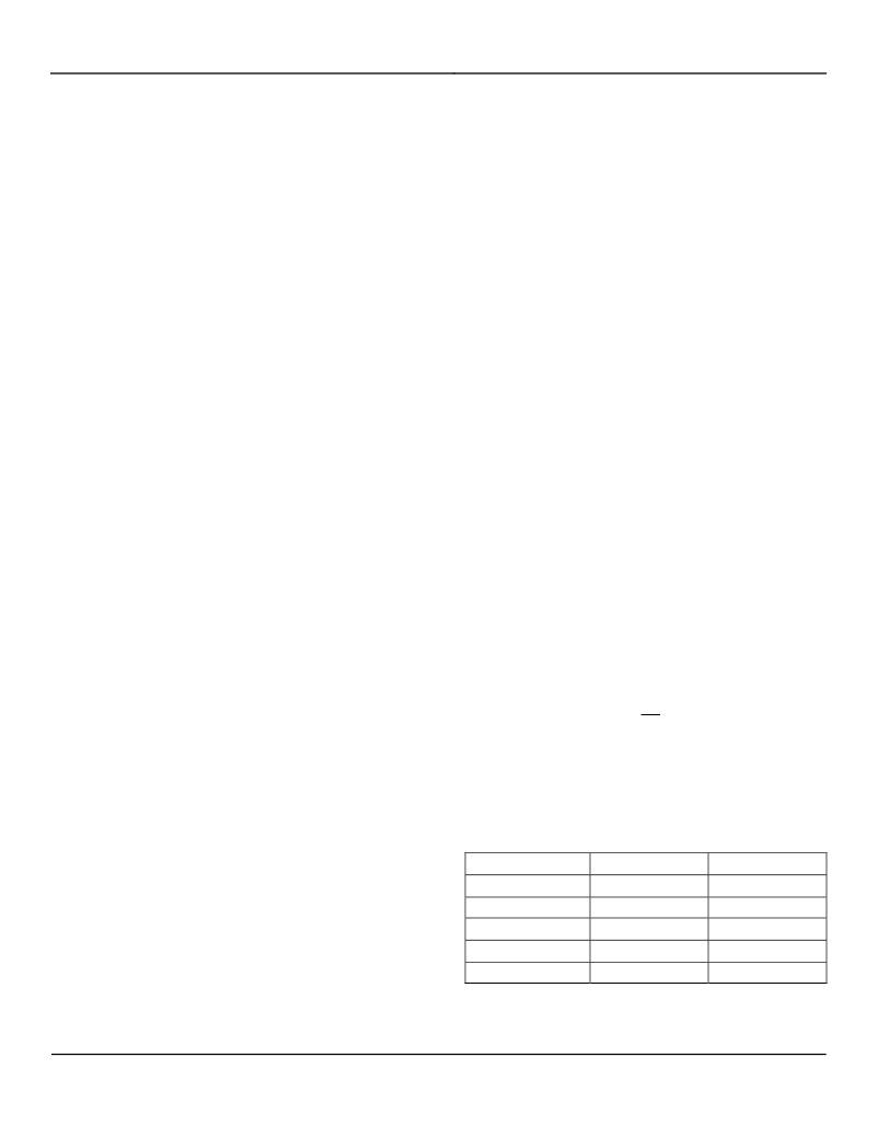
�The� output� voltage� can� be� programmed� between� 0.65V�
�and� 3.6V� using� the� following� equation:�
�V� OUT� =� V� REF� � ?� 1� +�
�?�
�AGND�
�The� analog� ground� (AGND)� is� the� ground� path� for� the�
�biasing� and� control� circuitry.� The� current� loop� for� the�
�?�
�?�
�R1� ?�
�R2� ?�
�signal� ground� should� be� separate� from� the� power� ground�
�(PGND)� loop.� Refer� to� the� layout� recommendations� for�
�more� details.�
�PGND�
�The� power� ground� pin� is� the� ground� path� for� the� high�
�where:�
�R1� is� the� top� resistor,� R2� is� the� bottom� resistor.�
�Example� feedback� resistor� values:�
�current� in� PWM� mode.� The� current� loop� for� the� power�
�ground� should� be� as� small� as� possible� and� separate�
�from� the� analog� ground� (AGND)� loop� as� applicable.�
�Refer� to� the� layout� recommendations� for� more� details.�
�September� 2010�
�10�
�V� OUT�
�1.2V�
�1.5V�
�1.8V�
�2.5V�
�3.3V�
�R1�
�274k�
�316k�
�301k�
�324k�
�309k�
�R2�
�294k�
�221k�
�158k�
�107k�
�71.5k�
�M9999-092910-A�
�相关PDF资料 |
PDF描述 |
|---|---|
| V24C3V3T75BF3 | CONVERTER MOD DC/DC 3.3V 75W |
| VI-JWV-CY | CONVERTER MOD DC/DC 5.8V 50W |
| EMM22DRUH | CONN EDGECARD 44POS DIP .156 SLD |
| V24C3V3T75BF2 | CONVERTER MOD DC/DC 3.3V 75W |
| VE-B3B-EX-B1 | CONVERTER MOD DC/DC 95V 75W |
相关代理商/技术参数 |
参数描述 |
|---|---|
| MIC33153YHJ | 制造商:Micrel 功能描述:Regulator 4MHz PWM 1.2A w/Inductor MLF14 |
| MIC33153YHJ TR | 功能描述:直流/直流开关调节器 4MHz PWM 1.2A Internal Inductor Buck Switcher with Soft-Start, Power Good & HyperLight Load RoHS:否 制造商:International Rectifier 最大输入电压:21 V 开关频率:1.5 MHz 输出电压:0.5 V to 0.86 V 输出电流:4 A 输出端数量: 最大工作温度: 安装风格:SMD/SMT 封装 / 箱体:PQFN 4 x 5 |
| MIC33153YHJ-EV | 功能描述:MIC33153 HyperLight Load? DC/DC, Step Down 1, Non-Isolated Outputs Evaluation Board 制造商:microchip technology 系列:HyperLight Load? 零件状态:有效 主要用途:DC/DC,步降 输出和类型:1,非隔离 功率 - 输出:- 电压 - 输出:1.8V 电流 - 输出:1.2A 电压 - 输入:2.7 V ~ 5.5 V 稳压器拓扑:降压 频率 - 开关:4MHz 板类型:完全填充 所含物品:板 使用的 IC/零件:MIC33153 标准包装:1 |
| MIC33153YHJ-TR | 功能描述:Buck Switching Regulator IC Positive Adjustable 0.62V 1 Output 1.2A 14-VFDFN Exposed Pad, 14-MLF? 制造商:microchip technology 系列:HyperLight Load? 包装:剪切带(CT) 零件状态:有效 功能:降压 输出配置:正 拓扑:降压 输出类型:可调式 输出数:1 电压 - 输入(最小值):2.7V 电压 - 输入(最大值):5.5V 电压 - 输出(最小值/固定):0.62V 电压 - 输出(最大值):3.6V 电流 - 输出:1.2A 频率 - 开关:4MHz 同步整流器:是 工作温度:-40°C ~ 125°C (TJ) 安装类型:表面贴装 封装/外壳:14-VFDFN 裸露焊盘,14-MLF? 供应商器件封装:14-MLF?(3x3.5) 标准包装:1 |
| MIC33163YGJ-T5 | 功能描述:Buck Switching Regulator IC Positive Adjustable 0.7V 1 Output 1A 20-PowerTFQFN 制造商:microchip technology 系列:HyperLight Load? 包装:剪切带(CT) 零件状态:停产 功能:降压 输出配置:正 拓扑:降压 输出类型:可调式 输出数:1 电压 - 输入(最小值):2.7V 电压 - 输入(最大值):5.5V 电压 - 输出(最小值/固定):0.7V 电压 - 输出(最大值):5V 电流 - 输出:1A 频率 - 开关:4MHz 同步整流器:是 工作温度:-40°C ~ 125°C (TJ) 安装类型:表面贴装 封装/外壳:20-PowerTFQFN 供应商器件封装:20-QFN(2.5x3) 标准包装:1 |
发布紧急采购,3分钟左右您将得到回复。