- 您现在的位置:买卖IC网 > PDF目录20457 > MIC4421ABM (Micrel Inc)IC DRIVER MOSFET 9A LS 8-SOIC PDF资料下载
参数资料
| 型号: | MIC4421ABM |
| 厂商: | Micrel Inc |
| 文件页数: | 7/13页 |
| 文件大小: | 0K |
| 描述: | IC DRIVER MOSFET 9A LS 8-SOIC |
| 标准包装: | 95 |
| 配置: | 低端 |
| 输入类型: | 反相 |
| 延迟时间: | 15ns |
| 电流 - 峰: | 9A |
| 配置数: | 1 |
| 输出数: | 1 |
| 电源电压: | 4.5 V ~ 18 V |
| 工作温度: | -40°C ~ 85°C |
| 安装类型: | 表面贴装 |
| 封装/外壳: | 8-SOIC(0.154",3.90mm 宽) |
| 供应商设备封装: | 8-SOIC |
| 包装: | 管件 |
�� �
�
�Micrel,� Inc.�
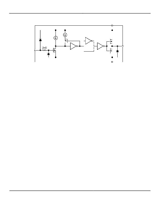
�Functional� Diagram�
�VS�
�MIC4421A/4422A�
�0.3mA�
�MIC4421A�
�INVERTING�
�IN�
�0.1mA�
�Q1�
�Q2�
�MIC4422A�
�NONINVERTING�
�Q3�
�Q4�
�OUT�
�GND�
�Figure� 4.� MIC4421A/22A� Block� Diagram�
�Functional� Description�
�Refer� to� the� functional� diagram.�
�The� MIC4422A� is� a� non-inverting� driver.� A� logic� high� on�
�the� IN� produces� gate� drive� output.� The� MIC4421A� is� an�
�inverting� driver.� A� logic� low� on� the� IN� produces� gate�
�drive� output.� The� output� is� used� to� turn� on� an� external� N-�
�channel� MOSFET.�
�Supply�
�V� S� (supply)� is� rated� for� +4.5V� to� +18V.� External�
�capacitors� are� recommended� to� decouple� noise.�
�Input�
�IN� (control)� is� a� TTL-compatible� input.� IN� must� be� forced�
�high� or� low� by� an� external� signal.� A� floating� input� will�
�cause� unpredictable� operation.�
�A� high� input� turns� on� Q1,� which� sinks� the� output� of� the�
�0.1mA� and� the� 0.3mA� current� source,� forcing� the� input� of�
�the� first� inverter� low.�
�Hysteresis�
�The� control� threshold� voltage,� when� IN� is� rising,� is�
�slightly� higher� than� the� control� threshold� voltage� when�
�CTL� is� falling.�
�When� IN� is� low,� Q2� is� on,� which� applies� the� additional�
�0.3mA� current� source� to� Q1.� Forcing� IN� high� turns� on� Q1�
�which� must� sink� 0.4mA� from� the� two� current� sources.�
�The� higher� current� through� Q1� causes� a� larger� drain-to-�
�source� voltage� drop� across� Q1.� A� slightly� higher� control�
�voltage� is� required� to� pull� the� input� of� the� first� inverter�
�down� to� its� threshold.�
�Q2� turns� off� after� the� first� inverter� output� goes� high.� This�
�reduces� the� current� through� Q1� to� 0.1mA.� The� lower�
�current� reduces� the� drain-to-source� voltage� drop� across�
�Q1.� A� slightly� lower� control� voltage� will� pull� the� input� of�
�the� first� inverter� up� to� its� threshold.�
�Drivers�
�The� second� (optional)� inverter� permits� the� driver� to� be�
�manufactured� in� inverting� and� non-inverting� versions.�
�The� last� inverter� functions� as� a� driver� for� the� output�
�MOSFETs� Q3� and� Q4.�
�Output�
�OUT� is� designed� to� drive� a� capacitive� load.� V� OUT� (output�
�voltage)� is� either� approximately� the� supply� voltage� or�
�approximately� ground,� depending� on� the� logic� state�
�applied� to� IN.�
�If� IN� is� high,� and� V� S� (supply)� drops� to� zero,� the� output�
�will� be� floating� (unpredictable).�
�June� 2007�
�7�
�M9999-062707�
�相关PDF资料 |
PDF描述 |
|---|---|
| R1D12-2415/H | CONV DC/DC 1W 24VIN +/-15VOUT |
| 345-010-500-802 | CARDEDGE 10POS DUAL .100 GREEN |
| M7WWK-5006R | D-SUB CABLE MFU50K/MC50M/MFU50K |
| 395-060-541-204 | CARD EDGE 60POS DL .100X.200 BLK |
| 395-060-541-202 | CARD EDGE 60POS DL .100X.200 BLK |
相关代理商/技术参数 |
参数描述 |
|---|---|
| MIC4421ABM TR | 功能描述:IC DRIVER MOSFET 9A LS 8-SOIC RoHS:否 类别:集成电路 (IC) >> PMIC - MOSFET,电桥驱动器 - 外部开关 系列:- 标准包装:50 系列:- 配置:高端 输入类型:非反相 延迟时间:200ns 电流 - 峰:250mA 配置数:1 输出数:1 高端电压 - 最大(自引导启动):600V 电源电压:12 V ~ 20 V 工作温度:-40°C ~ 125°C 安装类型:通孔 封装/外壳:8-DIP(0.300",7.62mm) 供应商设备封装:8-DIP 包装:管件 其它名称:*IR2127 |
| MIC4421ABN | 功能描述:IC DRIVER MOSFET 9A LS 8-DIP RoHS:否 类别:集成电路 (IC) >> PMIC - MOSFET,电桥驱动器 - 外部开关 系列:- 标准包装:50 系列:- 配置:高端 输入类型:非反相 延迟时间:200ns 电流 - 峰:250mA 配置数:1 输出数:1 高端电压 - 最大(自引导启动):600V 电源电压:12 V ~ 20 V 工作温度:-40°C ~ 125°C 安装类型:通孔 封装/外壳:8-DIP(0.300",7.62mm) 供应商设备封装:8-DIP 包装:管件 其它名称:*IR2127 |
| MIC4421ACM | 功能描述:IC DRIVER MOSFET 9A LS 8-SOIC RoHS:否 类别:集成电路 (IC) >> PMIC - MOSFET,电桥驱动器 - 外部开关 系列:- 标准包装:50 系列:- 配置:高端 输入类型:非反相 延迟时间:200ns 电流 - 峰:250mA 配置数:1 输出数:1 高端电压 - 最大(自引导启动):600V 电源电压:12 V ~ 20 V 工作温度:-40°C ~ 125°C 安装类型:通孔 封装/外壳:8-DIP(0.300",7.62mm) 供应商设备封装:8-DIP 包装:管件 其它名称:*IR2127 |
| MIC4421ACM TR | 功能描述:IC DRIVER MOSFET 9A LS 8-SOIC RoHS:否 类别:集成电路 (IC) >> PMIC - MOSFET,电桥驱动器 - 外部开关 系列:- 标准包装:50 系列:- 配置:高端 输入类型:非反相 延迟时间:200ns 电流 - 峰:250mA 配置数:1 输出数:1 高端电压 - 最大(自引导启动):600V 电源电压:12 V ~ 20 V 工作温度:-40°C ~ 125°C 安装类型:通孔 封装/外壳:8-DIP(0.300",7.62mm) 供应商设备封装:8-DIP 包装:管件 其它名称:*IR2127 |
| MIC4421ACN | 功能描述:IC DRIVER MOSFET 9A LS 8-DIP RoHS:否 类别:集成电路 (IC) >> PMIC - MOSFET,电桥驱动器 - 外部开关 系列:- 标准包装:50 系列:- 配置:高端 输入类型:非反相 延迟时间:200ns 电流 - 峰:250mA 配置数:1 输出数:1 高端电压 - 最大(自引导启动):600V 电源电压:12 V ~ 20 V 工作温度:-40°C ~ 125°C 安装类型:通孔 封装/外壳:8-DIP(0.300",7.62mm) 供应商设备封装:8-DIP 包装:管件 其它名称:*IR2127 |
发布紧急采购,3分钟左右您将得到回复。