- 您现在的位置:买卖IC网 > PDF目录20422 > MIC5013BM TR (Micrel Inc)IC DRIVER MOSF HI/LOW SIDE 8SOIC PDF资料下载
参数资料
| 型号: | MIC5013BM TR |
| 厂商: | Micrel Inc |
| 文件页数: | 6/15页 |
| 文件大小: | 0K |
| 描述: | IC DRIVER MOSF HI/LOW SIDE 8SOIC |
| 标准包装: | 2,500 |
| 配置: | 高端或低端 |
| 输入类型: | 非反相 |
| 延迟时间: | 60µs |
| 配置数: | 1 |
| 输出数: | 1 |
| 电源电压: | 7 V ~ 32 V |
| 工作温度: | -40°C ~ 85°C |
| 安装类型: | 表面贴装 |
| 封装/外壳: | 8-SOIC(0.154",3.90mm 宽) |
| 供应商设备封装: | 8-SOIC |
| 包装: | 带卷 (TR) |
| 其它名称: | MIC5013BMTR MIC5013BMTR-ND |
�� �
�
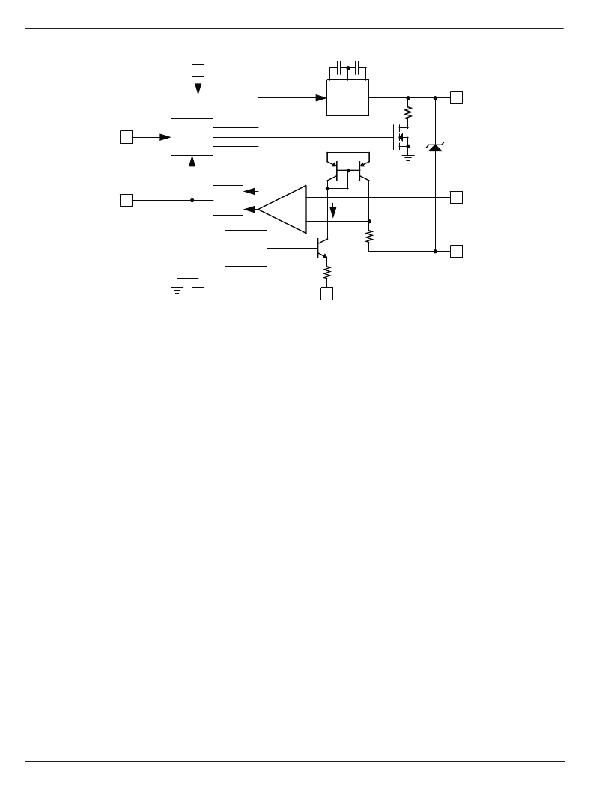
�MIC5013�
�Block� Diagram�
�V+�
�7�
�CHARGE�
�PUMP�
�500� ?�
�6� Gate�
�Micrel,� Inc.�
�Input� 1�
�LOGIC�
�CURRENT�
�SENSE�
�LATCH�
�MIC5013�
�V+�
�12.5V�
�Fault� 8�
�Q�
�R�
�S�
�+�
�–�
�I2�
�+�
�3� Sense�
�V.� REG�
�V� TR� I� P�
�–�
�1k�
�4� Source�
�1k�
�5�
�Ground�
�Applications� Information�
�Functional� Description� (refer� to� block� diagram� )�
�The� various� MIC5013� functions� are� controlled� via� a� logic�
�block� connected� to� the� input� pin� 1.� When� the� input� is� low,�
�all� functions� are� turned� off� for� low� standby� current� and� the�
�gate� of� the� power� MOSFET� is� also� held� low� through� 500Ω�
�to� an� N-channel� switch.� When� the� input� is� taken� above� the�
�turn-on� threshold� (3.5V� typical),� the� N-channel� switch� turns�
�off� and� the� charge� pump� is� turned� on� to� charge� the� gate� of�
�the� power� FET.� A� bandgap� type� voltage� regulator� is� also�
�turned� on� which� biases� the� current� sense� circuitry.�
�The� charge� pump� incorporates� a� 100kHz� oscillator� and�
�on-chip� pump� capacitors� capable� of� charging� 1nF� to� 5V�
�above� supply� in� 60μs� typical.� The� charge� pump� is� capable�
�of� pumping� the� gate� up� to� over� twice� the� supply� voltage.�
�For� this� reason,� a� zener� clamp� (12.5V� typical)� is� provided�
�between� the� gate� pin� 6� and� source� pin� 4� to� prevent� exceed-�
�ing� the� V� GS� rating� of� the� MOSFET� at� high� supplies.�
�The� current� sense� operates� by� comparing� the� sense� volt-�
�age� at� pin� 3� to� an� offset� version� of� the� source� voltage� at�
�pin� 4.� Current� I2� ?owing� in� threshold� pin� 2� is� mirrored� and�
�returned� to� the� source� via� a� 1k� resistor� to� set� the� offset,�
�or� trip� voltage.� When� (V� SENSE� –� V� SOURCE� )� exceeds� V� TRIP� ,�
�the� current� sense� trips� and� sets� the� current� sense� latch� to�
�turn� off� the� power� FET.� An� integrating� comparator� is� used�
�to� reduce� sensitivity� to� spikes� on� pin� 3.� The� latch� is� reset�
�to� turn� the� FET� back� on� by� “recycling”� the� input� pin� 1� low�
�and� then� high� again.�
�A� resistor� R� TH� from� pin� 2� to� ground� sets� I2,� and� hence� V� TRIP� .�
�An� additional� capacitor� C� TH� from� pin� 2� to� ground� creates� a�
�higher� trip� voltage� at� turn-on,� which� is� necessary� to� prevent�
�high� in-rush� current� loads� such� as� lamps� or� capacitors� from�
�false-tripping� the� current� sense.�
�2�
�Threshold�
�When� the� current� sense� has� tripped,� the� fault� pin� 8� will� be�
�high� as� long� as� the� input� pin� 1� remains� high.� However,� when�
�the� input� is� low� the� fault� pin� will� also� be� low.�
�Construction� Hints�
�High� current� pulse� circuits� demand� equipment� and� assembly�
�techniques� that� are� more� stringent� than� normal� low� current�
�lab� practices.� The� following� are� the� sources� of� pitfalls� most�
�often� encountered� during� prototyping:� Supplies:� many� bench�
�power� supplies� have� poor� transient� response.� Circuits� that�
�are� being� pulse� tested,� or� those� that� operate� by� pulse-width�
�modulation� will� produce� strange� results� when� used� with� a�
�supply� that� has� poor� ripple� rejection,� or� a� peaked� transient�
�response.� Monitor� the� power� supply� voltage� that� appears�
�at� the� drain� of� a� high-side� driver� (or� the� supply� side� of� the�
�load� in� a� low-side� driver)� with� an� oscilloscope.� It� is� not� un-�
�common� to� ?nd� bench� power� supplies� in� the� 1kW� class� that�
�overshoot� or� undershoot� by� as� much� as� 50%� when� pulse�
�loaded.� Not� only� will� the� load� current� and� voltage� measure-�
�ments� be� affected,� but� it� is� possible� to� over-stress� various�
�components—especially� electrolytic� capacitors—with� pos-�
�sibly� catastrophic� results.� A� 10μF� supply� bypass� capacitor�
�at� the� chip� is� recommended.�
�Residual� Resistances:� Resistances� in� circuit� connections�
�may� also� cause� confusing� results.� For� example,� a� circuit�
�may� employ� a� 50m� power� MOSFET� for� low� drop,� but�
�careless� construction� techniques� could� easily� add� 50� to�
�100m� resistance.� Do� not� use� a� socket� for� the� MOSFET.� If�
�the� MOSFET� is� a� TO-220� type� package,� make� high-current�
�drain� connections� to� the� tab.� Wiring� losses� have� a� profound�
�effect� on� high-current� circuits.� A� ?oating� millivoltmeter� can�
�identify� connections� that� are� contributing� excess� drop�
�under� load.�
�MIC5013�
�6�
�July� 2005�
�相关PDF资料 |
PDF描述 |
|---|---|
| MLK1005S3N9S | INDUCTOR MULTILAYER 3.9NH 0402 |
| SRN8040-330M | INDUCTOR POWER SHIELD 33UH SMD |
| EGM08DTKD | CONN EDGECARD 16POS DIP .156 SLD |
| ESC06DRXH-S734 | CONN EDGECARD 12POS DIP .100 SLD |
| SBG1640CT | DIODE SCHOTTKY CC 40V 16A D2-PAK |
相关代理商/技术参数 |
参数描述 |
|---|---|
| MIC5013BN | 功能描述:IC DRIVER MOSFET HI/LO SIDE 8IP RoHS:否 类别:集成电路 (IC) >> PMIC - MOSFET,电桥驱动器 - 外部开关 系列:- 标准包装:50 系列:- 配置:高端 输入类型:非反相 延迟时间:200ns 电流 - 峰:250mA 配置数:1 输出数:1 高端电压 - 最大(自引导启动):600V 电源电压:12 V ~ 20 V 工作温度:-40°C ~ 125°C 安装类型:通孔 封装/外壳:8-DIP(0.300",7.62mm) 供应商设备封装:8-DIP 包装:管件 其它名称:*IR2127 |
| MIC5013YM | 功能描述:功率驱动器IC High Side MOSFET Predriver - Lead Free RoHS:否 制造商:Micrel 产品:MOSFET Gate Drivers 类型:Low Cost High or Low Side MOSFET Driver 上升时间: 下降时间: 电源电压-最大:30 V 电源电压-最小:2.75 V 电源电流: 最大功率耗散: 最大工作温度:+ 85 C 安装风格:SMD/SMT 封装 / 箱体:SOIC-8 封装:Tube |
| MIC5013YM TR | 功能描述:功率驱动器IC High Side MOSFET Predriver - Lead Free RoHS:否 制造商:Micrel 产品:MOSFET Gate Drivers 类型:Low Cost High or Low Side MOSFET Driver 上升时间: 下降时间: 电源电压-最大:30 V 电源电压-最小:2.75 V 电源电流: 最大功率耗散: 最大工作温度:+ 85 C 安装风格:SMD/SMT 封装 / 箱体:SOIC-8 封装:Tube |
| MIC5013YN | 功能描述:功率驱动器IC High Side MOSFET Predriver - Lead Free RoHS:否 制造商:Micrel 产品:MOSFET Gate Drivers 类型:Low Cost High or Low Side MOSFET Driver 上升时间: 下降时间: 电源电压-最大:30 V 电源电压-最小:2.75 V 电源电流: 最大功率耗散: 最大工作温度:+ 85 C 安装风格:SMD/SMT 封装 / 箱体:SOIC-8 封装:Tube |
| MIC5014 | 制造商:MICREL 制造商全称:Micrel Semiconductor 功能描述:Low-Cost High- or Low-Side MOSFET Driver |
发布紧急采购,3分钟左右您将得到回复。