- 您现在的位置:买卖IC网 > Datasheet目录45 > MIC5158BN (Micrel Inc)IC REG CTRLR SGL FIX/ADJ 14-DIP Datasheet资料下载
参数资料
| 型号: | MIC5158BN |
| 厂商: | Micrel Inc |
| 文件页数: | 8/13页 |
| 文件大小: | 271K |
| 描述: | IC REG CTRLR SGL FIX/ADJ 14-DIP |
| 标准包装: | 25 |
| 类型: | 正,固定式或可调式 |
| 输出数: | 1 |
| 输出电压: | 5V,1.3 V ~ 36 V |
| 电流 - 电源: | 4.5mA |
| 输入电压: | 3 V ~ 36 V |
| 工作温度: | -40°C ~ 85°C |
| 封装/外壳: | 14-DIP(0.300",7.62mm) |
| 供应商设备封装: | 14-DIP |
| 包装: | 管件 |
MIC5156/5157/5158
Micrel, Inc.
MIC5156/5157/5158
8
August 2005
Charge Pump (MIC5157/5158 only)
The charge pump tripler creates a dc voltage across reservoir
capacitor C3. External capacitors C1 and C2 provide the nec-
essary storage for the stages of the charge pump tripler.
The triplers approximate dc output voltage is:
V
CP
H 3 (V
DD
1)
where:
V
CP
= charge pump output voltage
V
DD
= supply voltage
The V
CP
clamp circuit limits the charge pump voltage to 16V
above V
DD
by gating the charge pump oscillator ON or OFF as
required. The charge pump oscillator operates at 160kHz.
The error amplier uses the charge pump voltage to drive
the gate of the external MOSFET. It provides a constant load
of about 1mA to the charge pump. The error amplier output
can swing to within 1V of V
CP
.
Although the MIC5157/8 is designed to provide gate drive
using its internal charge pump, an external gate drive sup-
ply voltage can be applied to V
CP
. When using an external
gate drive supply, V
CP
must not be forced more than 14V
higher than V
DD
.
When constant loads are driven, the ON/OFF switching of
the charge pump may be evident on the output waveform.
This is caused by the charge pump switching ON and rapidly
increasing the supply voltage to the error amplier. The period
of this small charge pump excitation is determined by a number
of factors: the input voltage, the 1mA op-amp load, any dc
leakage associated with the MOSFET gate circuit, the size
of the charge pump capacitors, the size of the charge pump
reservoir capacitor, and the characteristics of the input voltage
and load. The period is lengthened by increasing the charge
pump reservoir capacitor (C3). The amplitude is reduced by
weakening the charge pumpthis is accomplished by reduc-
ing the size of the pump capacitors (C1 and C2). If this small
burst is a problem in the application, use a 10礔 reservoir
capacitor at C3 and 0.01礔 pump capacitors at C1 and C2.
Note that the recovery time to repetitive load transients may
be affected with small pump capacitors.
Gate-to-Source Clamp
A gate-to-source protective voltage clamp of 16.6V protects
the MOSFET in the event that the output voltage is suddenly
forced to zero volts. This prevents damage to the external
MOSFET during shorted load conditions. Refer to
Charge
Pump
for normal clamp circuit operation.
The source connection required by the gate-to-source clamp
is not available on the adjustable version of the MIC5156.
Output Regulation
At start-up, the error amplier feedback voltage (EA), or
internal feedback on xed versions, is below nominal when
compared to the internal 1.235V bandgap reference. This
forces the error amplier output high which turns on exter-
nal MOSFET Q1. Once the output reaches regulation, the
controller maintains constant output voltage under changing
input and load conditions by adjusting the error amplier
output voltage (gate enhancement voltage) according to the
feedback voltage.
Out-of-Regulation Detection
When the output voltage is 8% or more below nominal, the
open-collector FLAG output (normally high) is forced low to
signal a fault condition. The FLAG output can be used to
signal or control external circuitry. The FLAG output can also
be used to shut down the regulator using the EN control.
Current Limiting
Super LDO Regulators perform constant-current limiting (not
foldback). To implement current limiting, a sense resistor
(R
S
) must be placed in the
power
path between V
DD
and
D (drain).
If the voltage drop across the sense resistor reaches 35mV,
the current limit comparator reduces the error amplier out-
put. The error amplier output is decreased only enough to
reduce the output current, keeping the voltage across the
sense resistor from exceeding 35mV.
Application Information
MOSFET Selection
Standard N-channel enhancement-mode MOSFETs are ac-
ceptable for most Super LDO regulator applications.
Logic-level N-channel enhancement-mode MOSFETs may
be necessary if the external gate drive voltage is too low
(MIC5156), or the input voltage is too low, to provide adequate
charge pump voltage (MIC5157/8) to enhance a standard
MOSFET.
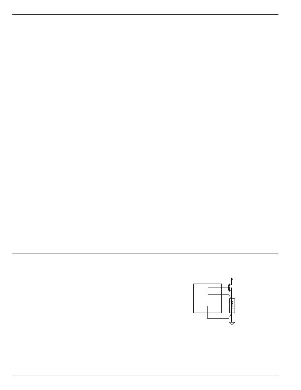
Circuit Layout
For the best voltage regulation, place the source, ground,
and error amplier connections as close as possible to the
load. See gures (1a) and (1b).
GND
S
G
MIC515x
V
IN
Figure 1a. Connections for Fixed Output
相关PDF资料 |
PDF描述 |
|---|---|
| MIC5159BM6 TR | IC REG CTRLR SGL POS ADJ SOT23-6 |
| MIC5190BMM TR | IC REG CTRLR SGL POS ADJ 10-MSOP |
| MIC5191BMM TR | IC REG CTRLR SGL POS ADJ 10-MSOP |
| ML4800CP | IC PFC CTRLR AVERAGE CURR 16DIP |
| ML4824CS2 | IC PFC PWM CTRLR COMBO 16-SOIC |
相关代理商/技术参数 |
参数描述 |
|---|---|
| MIC5158YM | 功能描述:低压差控制器 - LDO Super LDO Regulator-5 volt/adj -(Lead Free) RoHS:否 制造商:Micrel 最大输入电压:5.5 V 输出电压:Adjustable 输出电流:10 mA 负载调节: 输出类型:Adjustable, Fixed 输出端数量:1 最大工作温度:+ 125 C 安装风格:SMD/SMT 封装 / 箱体:SOT-23-6 |
| MIC5158YM TR | 功能描述:低压差控制器 - LDO Super LDO Regulator-5 volt/adj -(Lead Free) RoHS:否 制造商:Micrel 最大输入电压:5.5 V 输出电压:Adjustable 输出电流:10 mA 负载调节: 输出类型:Adjustable, Fixed 输出端数量:1 最大工作温度:+ 125 C 安装风格:SMD/SMT 封装 / 箱体:SOT-23-6 |
| MIC5158YM | 制造商:Micrel Inc 功能描述:IC VOLTAGE REGULATOR |
| MIC5158YM | 制造商:Micrel Inc 功能描述:Linear Voltage Regulator IC |
| MIC5158YN | 功能描述:低压差控制器 - LDO Super LDO Regulator-5 volt/adj -(Lead Free) RoHS:否 制造商:Micrel 最大输入电压:5.5 V 输出电压:Adjustable 输出电流:10 mA 负载调节: 输出类型:Adjustable, Fixed 输出端数量:1 最大工作温度:+ 125 C 安装风格:SMD/SMT 封装 / 箱体:SOT-23-6 |
发布紧急采购,3分钟左右您将得到回复。