- 您现在的位置:买卖IC网 > PDF目录19672 > MIC5207-3.3BZ (Micrel Inc)IC REG LDO 3.3V .18A TO92-3 PDF资料下载
参数资料
| 型号: | MIC5207-3.3BZ |
| 厂商: | Micrel Inc |
| 文件页数: | 9/13页 |
| 文件大小: | 0K |
| 描述: | IC REG LDO 3.3V .18A TO92-3 |
| 标准包装: | 500 |
| 稳压器拓扑结构: | 正,固定式 |
| 输出电压: | 3.3V |
| 输入电压: | 最高 16V |
| 电压 - 压降(标准): | 0.165V @ 150mA |
| 稳压器数量: | 1 |
| 电流 - 输出: | 180mA |
| 工作温度: | -40°C ~ 125°C |
| 安装类型: | 通孔 |
| 封装/外壳: | TO-226-3、TO-92-3 标准主体 |
| 供应商设备封装: | TO-92-3 |
| 包装: | 管件 |
�� �
�
�(� T� J(MAX)� ?� T� A� )�
�Micrel,� Inc.�
�Application� Information�
�Enable/Shutdown�
�Forcing� EN� (enable/shutdown)� high� (>� 2V)� enables� the�
�regulator.� EN� is� compatible� with� CMOS� logic� gates.�
�If� the� enable/shutdown� feature� is� not� required,� connect�
�EN� (pin� 3)� to� IN� (supply� input,� pin� 1).� See� Figure� 1.�
�Input� Capacitor�
�A� 1μF� capacitor� should� be� placed� from� IN� to� GND� if�
�there� is� more� than� 10� inches� of� wire� between� the� input�
�and� the� ac� filter� capacitor� or� if� a� battery� is� used� as� the�
�input.�
�Reference� Bypass� Capacitor�
�BYP� (reference� bypass)� is� connected� to� the� internal�
�voltage� reference.� A� 470pF� capacitor� (C� BYP� )� connected�
�from� BYP� to� GND� quiets� this� reference,� providing� a�
�significant� reduction� in� output� noise.� CBYP� reduces� the�
�regulator� phase� margin;� when� using� CBYP,� output�
�capacitors� of� 2.2μF� or� greater� are� generally� required� to�
�maintain� stability.�
�MIC5207�
�No-Load� Stability�
�The� MIC5207� will� remain� stable� and� in� regulation� with� no�
�load� (other� than� the� internal� voltage� divider)� unlike� many�
�other� voltage� regulators.� This� is� especially� important� in�
�CMOSRAM� keep-alive� applications.�
�Thermal� Considerations�
�The� MIC5207� is� designed� to� provide� 180mA� of�
�continuous� current� in� a� very� small� package.� Maximum�
�power� dissipation� can� be� calculated� based� on� the� output�
�current� and� the� voltage� drop� across� the� part.� To�
�determine� the� maximum� power� dissipation� of� the�
�package,� use� the� junction-to-ambient� thermal� resistance�
�of� the� device� and� the� following� basic� equation:�
�P� D(MAX)� =�
�θ� JA�
�T� J(max)� is� the� maximum� junction� temperature� of� the� die,�
�125°C,� and� T� A� is� the� ambient� operating� temperature.� θ� JA�
�is� layout� dependent;� Table� 1� shows� examples� of�
�junction-to-ambient� thermal� resistance� for� the� MIC5207.�
�The� start-up� speed� of� the� MIC5207� is� inversely�
�proportional� to� the� size� of� the� reference� bypass�
�capacitor.� Applications� requiring� a� slow� ramp-up� of�
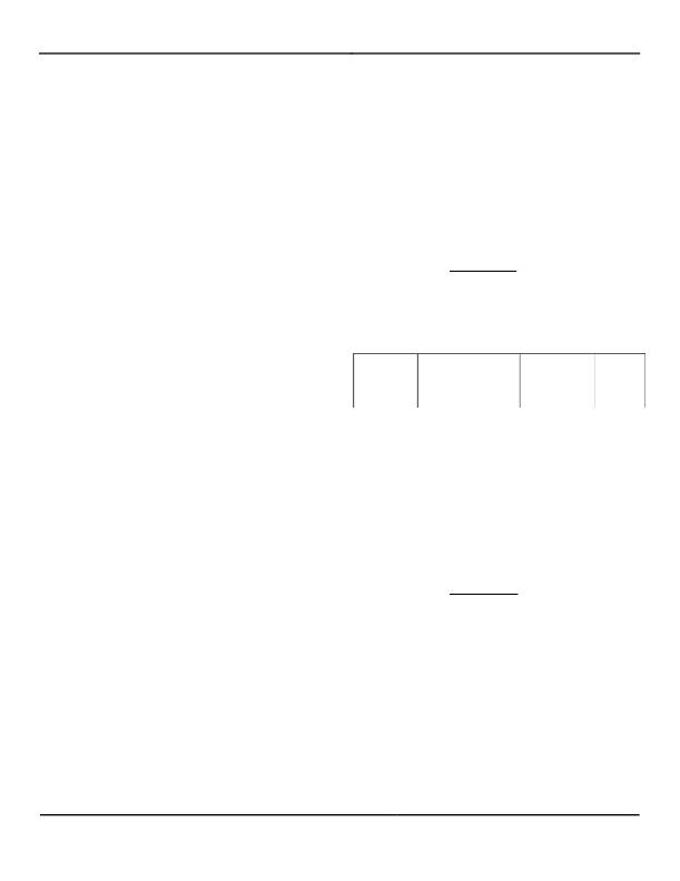
�Package�
�SOT-23-5�
�θ� JA� Recommemded�
�Minimum� Footprint�
�235°C/W�
�θ� JA� 1”� Square�
�Copper� Clad�
�170°C/W�
�θ� J/C�
�130°C/W�
�output� voltage� should� consider� larger� values� of� C� BYP� .�
�Likewise,� if� rapid� turn-on� is� necessary,� consider� omitting�
�C� BYP� .�
�(M5)�
�Table� 1.� SOT-23-5� Thermal� Resistance�
�P� D(MAX)� =�
�If� output� noise� is� not� a� major� concern,� omit� C� BYP� and�
�leave� BYP� open.�
�Output� Capacitor�
�An� output� capacitor� is� required� between� OUT� and� GND�
�to� prevent� oscillation.� The� minimum� size� of� the� output�
�capacitor� is� dependent� upon� whether� a� reference� bypass�
�capacitor� is� used.� 1.0μF� minimum� is� recommended�
�when� CBYP� is� not� used� (see� Figure� 2).� 2.2μF� minimum�
�is� recommended� when� C� BYP� is� 470pF� (see� Figure� 1).�
�Larger� values� improve� the� regulator’s� transient�
�response.� The� output� capacitor� value� may� be� increased�
�without� limit.�
�The� output� capacitor� should� have� an� ESR� (effective�
�series� resistance)� of� about� 5� ?� or� less� and� a� resonant�
�frequency� above� 1MHz.� Ultra-low-ESR� capacitors� can�
�cause� a� low� amplitude� oscillation� on� the� output� and/or�
�under-damped� transient� response.� Most� tantalum� or�
�aluminum� electrolytic� capacitors� are� adequate;� film� types�
�will� work,� but� are� more� expensive.� Since� many� aluminum�
�electrolytics� have� electrolytes� that� freeze� at� about�
�–30°C,� solid� tantalums� are� recommended� for� operation�
�below� –25°C.�
�At� lower� values� of� output� current,� less� output�
�capacitance� is� required� for� output� stability.� The� capacitor�
�can� be� reduced� to� 0.47μF� for� current� below� 10mA� or�
�0.33μF� for� currents� below� 1mA.�
�The� actual� power� dissipation� of� the� regulator� circuit� can�
�be� determined� using� the� equation:�
�P� D� =� (� V� IN� ?� V� OUT� )� I� OUT� +� V� IN� I� GND�
�Substituting� P� D(max)� for� P� D� and� solving� for� the� operating�
�conditions� that� are� critical� to� the� application� will� give� the�
�maximum� operating� conditions� for� the� regulator� circuit.�
�For� example,� when� operating� the� MIC5207-3.3BM5� at�
�room� temperature� with� a� minimum� footprint� layout,� the�
�maximum� input� voltage� for� a� set� output� current� can� be�
�determined� as� follows:�
�125� °� C� ?� 25� °� C�
�235�
�P� D(MAX)� =� 425mW�
�The� junction-to-ambient� thermal� resistance� for� the�
�minimum� footprint� is� 220°C/W,� from� Table� 1.� The�
�maximum� power� dissipation� must� not� be� exceeded� for�
�proper� operation.� Using� the� output� voltage� of� 3.3V� and�
�an� output� current� of� 150mA,� the� maximum� input� voltage�
�can� be� determined.� From� the� Electrical� Characteristics�
�table,� the� maximum� ground� current� for� 150mA� output�
�current� is� 3000μA� or� 3mA.�
�455mW� =� (� V� IN� ?� 3.3� )� 150mA� +� V� IN� ?� 3mA�
�455mW� =� V� IN� ?� 150mA� -� 495mW� +� V� IN� ?� 3mA�
�920mW� =� V� IN� ?� 153mA�
�December� 2007�
�9�
�M9999-123107�
�相关PDF资料 |
PDF描述 |
|---|---|
| TMK107SD392KA-T | CAP CER 3900PF 25V 10% 0603 |
| 180-M15-203L021 | CONN DB15 FMAL HD SLD CUP NICKEL |
| ACC26DRYI-S93 | CONN EDGECARD 52POS DIP .100 SLD |
| HSC31DRYS-S734 | CONN EDGECARD 62POS DIP .100 SLD |
| 180-M15-203L011 | CONN DB15 FMAL HD SLD CUP NICKEL |
相关代理商/技术参数 |
参数描述 |
|---|---|
| MIC5207-4.0BM5 | 制造商:Rochester Electronics LLC 功能描述:- Bulk |
| MIC5207-4.0BM5 TR | 功能描述:IC REG LDO 4V .18A SOT23-5 RoHS:否 类别:集成电路 (IC) >> PMIC - 稳压器 - 线性 系列:- 标准包装:500 系列:- 稳压器拓扑结构:正,固定式 输出电压:12V 输入电压:14.5 V ~ 35 V 电压 - 压降(标准):- 稳压器数量:1 电流 - 输出:500mA 电流 - 限制(最小):- 工作温度:-40°C ~ 125°C 安装类型:通孔 封装/外壳:TO-205AD,TO-39-3 金属罐 供应商设备封装:TO-39 包装:散装 其它名称:*LM78M12CH*LM78M12CH/NOPBLM78M12CH |
| MIC5207-4.0BM5TR | 制造商:RF Micro Devices Inc 功能描述: |
| MIC5207-4.0YM5 | 制造商:MICREL 制造商全称:Micrel Semiconductor 功能描述:180mA Low-Noise LDO Regulator |
| MIC5207-4.0YM5 TR | 功能描述:低压差稳压器 - LDO 180mA 3% Low Noise LDO(Lead Free) RoHS:否 制造商:Texas Instruments 最大输入电压:36 V 输出电压:1.4 V to 20.5 V 回动电压(最大值):307 mV 输出电流:1 A 负载调节:0.3 % 输出端数量: 输出类型:Fixed 最大工作温度:+ 125 C 安装风格:SMD/SMT 封装 / 箱体:VQFN-20 |
发布紧急采购,3分钟左右您将得到回复。