参数资料
| 型号: | MIC7122YMM |
| 厂商: | Micrel Inc |
| 文件页数: | 6/8页 |
| 文件大小: | 0K |
| 描述: | IC OPAMP R-R DUAL 8-MSOP |
| 标准包装: | 100 |
| 系列: | MM8™ |
| 放大器类型: | 通用 |
| 电路数: | 2 |
| 输出类型: | 满摆幅 |
| 转换速率: | 0.5 V/µs |
| 增益带宽积: | 420kHz |
| 电流 - 输入偏压: | 1pA |
| 电压 - 输入偏移: | 500µV |
| 电流 - 电源: | 900µA |
| 电流 - 输出 / 通道: | 250mA |
| 电压 - 电源,单路/双路(±): | 2.2 V ~ 15 V,±1.1 V ~ 7.5 V |
| 工作温度: | -40°C ~ 85°C |
| 安装类型: | 表面贴装 |
| 封装/外壳: | 8-TSSOP,8-MSOP(0.118",3.00mm 宽) |
| 供应商设备封装: | 8-MSOP |
| 包装: | 管件 |
MIC7122
Micrel
MIC7122
6
June 2005
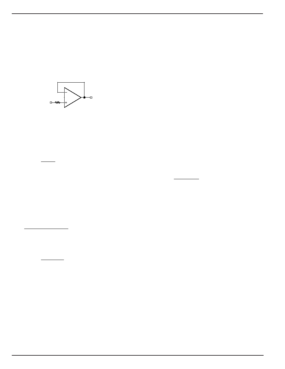
Application Information
Input Common-Mode Voltage
The MIC7122 tolerates input overdrive by at least 300mV
beyond either rail without producing phase inversion.
If the absolute maximum input voltage is exceeded, the input
current should be limited to
±5mA maximum to prevent
reducing reliability. A 10k
series input resistor, used as a
current limiter, will protect the input structure from voltages as
large as 50V above the supply or below ground. See Figure
1.
VIN
VOUT
10k
RIN
Figure 1. Input Current-Limit Protection
Output Voltage Swing
Sink and source output resistances of the MIC7122 are
equal. Maximum output voltage swing is determined by the
load and the approximate output resistance. The output
resistance is:
R
V
I
OUT
DROP
LOAD
=
V
DROP is the voltage dropped within the amplifier output
stage. V
DROP and ILOAD can be determined from the VO
(output swing) portion of the appropriate Electrical Character-
istics table. I
LOAD is equal to the typical output high voltage
minus V+/2 and divided by R
LOAD. For example, using the
Electrical Characteristics DC (5V) table, the typical output
high voltage drops 13mV using a 2k
load (connected to V+/
2), which produces an I
LOAD of:
Because of output stage symmetry, the corresponding typical
output low voltage (13mV) also equals V
DROP. Then:
Power Dissipation
The MIC7122 output drive capability requires considering
power dissipation. If the load impedance is low, it is possible
to damage the device by exceeding the 125
°C junction
temperature rating.
On-chip power consists of two components: supply power
and output stage power. Supply power (P
S) is the product of
the supply voltage (V
S = VV+ – VV–) and supply current (IS).
Output stage power (P
O) is the product of the output stage
voltage drop (V
DROP) and the output (load) current (IOUT).
Total on-chip power dissipation is:
P
D = PS + PO
P
D = VS IS + VDROP IOUT
where:
P
D = total on-chip power
P
S = supply power dissipation
P
O = output power dissipation
V
S = VV+ – VV–
I
S = power supply current
V
DROP = VV+ – VOUT
(sourcing current)
V
DROP = VOUT – VV–
(sinking current)
The above addresses only steady state (dc) conditions. For
non-dc conditions the user must estimate power dissipation
based on rms value of the signal.
The task is one of determining the allowable on-chip power
dissipation for operation at a given ambient temperature and
power supply voltage. From this determination, one may
calculate the maximum allowable power dissipation and,
after subtracting P
S, determine the maximum allowable load
current, which in turn can be used to determine the miniumum
load impedance that may safely be driven. The calculation is
summarized below.
P
TT
D(max)
J(max)
A
JA
=
θ
JA(MSOP-8) = 200°C/W
Driving Capacitive Loads
Driving a capacitive load introduces phase-lag into the output
signal, and this in turn reduces op-amp system phase margin.
The application that is least forgiving of reduced phase
margin is a unity gain amplifier. The MIC7122 can typically
drive a 200pF capacitive load connected directly to the output
when configured as a unity-gain amplifier and powered with
a 2.2V supply. At 15V operation the circuit typically drives
500pF.
Using Large-Value Feedback Resistors
A large-value feedback resistor (> 500k
) can reduce the
phase margin of a system. This occurs when the feedback
resistor acts in conjunction with input capacitance to create
phase lag in the feedback signal. Input capacitance is usually
a combination of input circuit components and other parasitic
capacitance, such as amplifier input capacitance and stray
printed circuit board capacitance.
Figure 2 illustrates a method of compensating phase lag
caused by using a large-value feedback resistor. Feedback
capacitor C
FB introduces sufficient phase lead to overcome
the phase lag caused by feedback resistor R
FB and input
5.0V – 0.013V – 2.5V
2k
1.244mA
=
R
0.013V
0.001244A
OUT == 10 5
.
相关PDF资料 |
PDF描述 |
|---|---|
| B24B-XADSS-N | CONN HDR XAD 24POS 2.5MM TIN TE |
| ADA4691-2ACPZ-RL | IC OPAMP GP R-R 3.6MHZ 10LFCSP |
| 626035-1 | CONN RING UNINS 10-11AWG |
| ADA4691-2ACBZ-RL | IC OPAMP GP R-R 3.6MHZ LP 9WLCSP |
| 51915-050 | PWRBLADE 3ACP+24S+2P R/A RECEPT |
相关代理商/技术参数 |
参数描述 |
|---|---|
| MIC7122YMM TR | 功能描述:运算放大器 - 运放 Dual CMOS Op Amp - Lead Free RoHS:否 制造商:STMicroelectronics 通道数量:4 共模抑制比(最小值):63 dB 输入补偿电压:1 mV 输入偏流(最大值):10 pA 工作电源电压:2.7 V to 5.5 V 安装风格:SMD/SMT 封装 / 箱体:QFN-16 转换速度:0.89 V/us 关闭:No 输出电流:55 mA 最大工作温度:+ 125 C 封装:Reel |
| MIC7122YMM-TR | 功能描述:General Purpose Amplifier 2 Circuit Rail-to-Rail 8-MSOP 制造商:microchip technology 系列:MM8?? 包装:剪切带(CT) 零件状态:有效 放大器类型:通用 电路数:2 输出类型:满摆幅 压摆率:0.5 V/μs 增益带宽积:420kHz -3db 带宽:- 电流 - 输入偏置:1pA 电压 - 输入失调:500μV 电流 - 电源:900μA 电流 - 输出/通道:250mA 电压 - 电源,单/双(±):2.2 V ~ 15 V,±1.1 V ~ 7.5 V 工作温度:-40°C ~ 85°C 安装类型:表面贴装 封装/外壳:8-TSSOP,8-MSOP(0.118",3.00mm 宽) 供应商器件封装:8-MSOP 标准包装:1 |
| MIC7201 | 制造商:MICREL 制造商全称:Micrel Semiconductor 功能描述:GainBlock⑩ Difference Amplifier Preliminary Information |
| MIC7201BM5 | 制造商:Rochester Electronics LLC 功能描述:- Bulk |
| MIC7211 | 制造商:MICREL 制造商全称:Micrel Semiconductor 功能描述:IttyBitty⑩ Rail-to-Rail Input Comparator Preliminary Information |
发布紧急采购,3分钟左右您将得到回复。