参数资料
| 型号: | MIC9130BQS |
| 厂商: | Micrel Inc |
| 文件页数: | 14/19页 |
| 文件大小: | 0K |
| 描述: | IC CTRLR DC-DC PWM HV HS 16-QSOP |
| 标准包装: | 98 |
| 应用: | 控制器,电信 |
| 输入电压: | 9 V ~ 18 V |
| 输出数: | 1 |
| 输出电压: | 4.7 V ~ 5 V |
| 工作温度: | -40°C ~ 125°C |
| 安装类型: | 表面贴装 |
| 封装/外壳: | 16-SSOP(0.154",3.90mm 宽) |
| 供应商设备封装: | 16-QSOP |
| 包装: | 管件 |
�� �
�
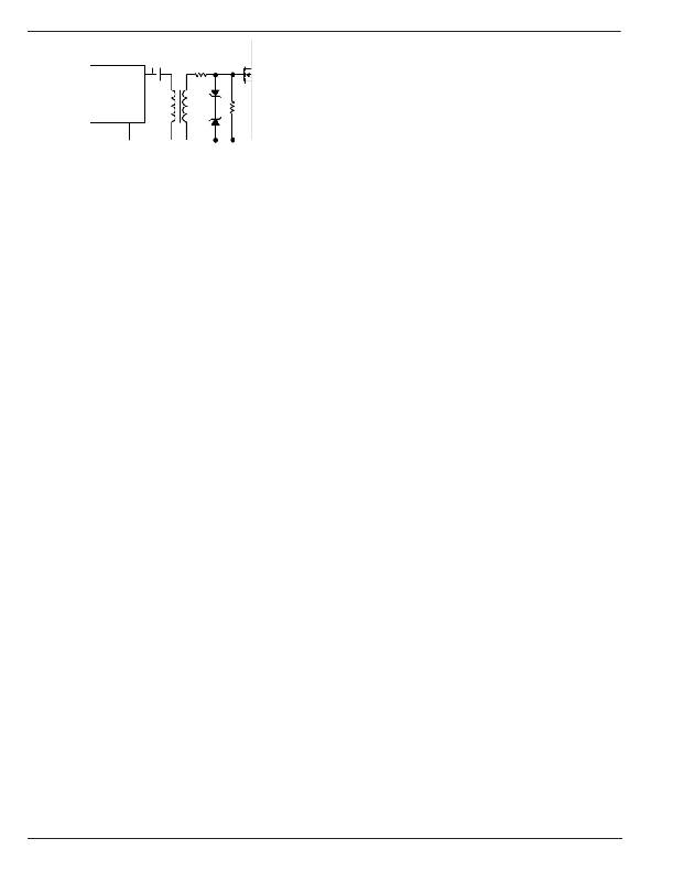
�MIC9130�
�Current� Sense� Circuit�
�Micrel,� Inc.�
�C1�
�T1�
�R1�
�The� current� sense� input� of� the� MIC9130� has� three� unique�
�features,� which� are� advantageous� in� a� high� speed,� high� ef-�
�Gate� Drive�
�Output�
�GND�
�1:N�
�D2�
�D1�
�R2�
�?� ciency� power� supply.�
�1.� The� overcurrent� threshold� is� nominally� 0.82V� instead�
�of� the� typical� 1.0V� found� in� most� switching� control�
�ICs.�
�2.� The� current� sense� pin� sources� a� nominal� 40� μ� A� of�
�Q� G�
�I� PK� =� 2� �
�I� PK� =�
�=� 2� .� 4� A�
�Figure 10�
�The� gate� impedance� of� a� MOSFET� is� capacitive� and� the�
�power� required� to� drive� the� gate� is� proportional� to� the� charge�
�required� to� turn� on� the� MOSFET,� the� peak� gate� voltage� and�
�the� switching� frequency.� Assuming� the� total� gate� charge� for�
�turn� on� and� turn� off� is� equal,� the� power� used� to� switch� the�
�MOSFET� on� and� off� is:�
�P� DRIVE� =� Q� G� � V� GS� � f� S�
�where:� Q� G� is� the� total� gate� charge� at� V� GS�
�V� GS� is� the� gate� to� source� voltage� of� the� MOSFET�
�usually� equal� to� V� CC�
�f� S� is� the� output� switching� frequency�
�The� power� required� to� drive� the� MOSFET� is� dissipated� in� the�
�drive� circuitry� of� the� MIC9130.� This� power� must� not� cause�
�the� die� temperature� to� exceed� the� maximum� rated� junction�
�temperature� of� 125� degrees� C.�
�MOSFET� Driver� IC’s� are� used� when� the� drive� requirement� for�
�the� MOSFETs� is� greater� than� the� capability� of� the� MIC9130�
�gate� drive� output.� While� the� peak� current� of� the� MIC9130�
�gate� drive� is� typically� 1.2A� at� V� IN� =12V,� a� gate� driver� ICs�
�will� sink� or� source� between� 1.2A� and� 12A� of� peak� current.�
�The� higher� peak� current� allows� faster� rise� and� fall� times� for�
�larger� MOSFETs.�
�The� drive� requirements� for� selecting� a� MOSFET� driver� are�
�determined� using� the� following� equation:�
�t�
�where:� Q� G� is� the� total� gate� charge� required� to� turn� on�
�the� MOSFET� at� a� speci� ?� ed� I� D� ,� V� G� and� V� DS� .� This�
�information� is� usually� given� in� the� MOSFET�
�speci� ?� cation� sheet.�
�t� is� the� gate� voltage� transition� time� (risetime� or� fall�
�time)�
�I� PK� is� the� peak� current� requirement� of� the�
�MOSFET� driver� IC.�
�For� example,� if� a� MOSFET� is� chosen� with� a� Q� G� of� 60nC� and�
�it� is� desired� to� have� a� 50nS� gate� to� source� risetime/falltime,�
�the� peak� current� requirement� of� the� MOSFET� driver� is:�
�2 × 60nC�
�50� ns�
�A� driver� such� as� the� MIC4424� will� meet� this� requirement.�
�For� more� information� on� choosing� a� MOSFET� driver,� see�
�the� Micrel� application� note� AN-24,� “� Designing� with� Low� Side�
�MOSFET� Drivers� .”�
�current� out� of� the� pin.� This� is� used� to� raise� the� current�
�limit� threshold� of� the� pin,� which� allows� a� smaller�
�current� sense� resistor� to� be� used.� This� improves� the�
�ef� ?� ciency� of� the� power� supply,� especially� in� lower�
�current� applications.�
�3.� The� delay� from� the� current� sense� input� to� the� output�
�is� typically� 50ns.�
�The� current� limit� threshold� of� the� ISNS� pin� was� set� at� 0.82V,�
�allowing� the� use� of� a� smaller� current� sense� resistor.� A� stable,�
�bandgap� derived� 40� μ� A� current� is� sourced� from� the� ISNS� pin.�
�A� voltage� drop� across� a� series� resistor� placed� between� the�
�pin� and� the� current� sense� resistor� level� increases� the� current�
�sense� signal� at� the� ISNS� pin.� This� allows� the� use� of� a� smaller�
�current� sense� resistor� if� the� full� 0.82V� peak� to� peak� current�
�signal� is� not� required.� Decreasing� the� value� of� the� current�
�sense� resistor� decreases� the� power� dissipation� in� the� resistor,�
�which� improves� the� ef� ?� ciency� of� the� power� supply.�
�The� delay� between� the� input� of� the� overcurrent� comparator�
�and� the� output� gate� drive� is� nominally� 50ns.� This� very� fast�
�response� time� allows� the� MIC9130� to� operate� at� higher� fre-�
�quencies� and� still� have� adequate� overcurrent� protection.�
�The� operation� of� the� current� sense� input� is� as� follows.� The�
�sensed� current� in� the� power� supply� is� converted� to� a� volt-�
�age� by� a� resistor� or� current� sense� transformer.� Referring� to�
�Figure� 1,� this� voltage� is� compared� to� the� output� of� the� error�
�ampli� ?� er,� which� sets� the� duty� cycle� of� the� gate� drive� output.�
�The� current� signal� is� also� connected� to� an� Imax� comparator.�
�Comparing� the� current� sense� signal� to� the� reference� voltage�
�sets� a� maximum� current� limit.� If� the� maximum� amplitude� of� the�
�current� sense� signal� exceeds� the� reference,� the� comparator�
�terminates� the� gate� drive� output� pulse.� It� aslo� discharges� the�
�soft� start� capacitor� when� the� CPWR� pin� is� high.�
�Leading� Edge� Current� Spike�
�The� current� signal� in� a� power� circuit� will� often� have� a� leading�
�edge� spike� caused� by� leakage� inductance,� parasitic� induc-�
�tance� and� capacitance,� diode� reverse� recovery� effects� and�
�snubbers.� These� spikes� can� cause� premature� termination� of�
�the� switching� cycle� if� they� are� not� eliminated.�
�A� resistor� may� be� added� in� series� between� the� current� sense�
�resistor� and� the� Isns� input.� The� input� and� board� trace� ca-�
�pacitance� of� the� ISNS� pin� (pin� 14)� is� approximately� 25pF.� A�
�1k� resistor� is� a� good� choice,� since� it� attenuates� most� of� the�
�ripple� without� distorting� the� current� sense� waveform.� It� has�
�a� minimal� effect� on� level,� offsetting� the� current� sense� signal�
�by� only� 40mV.�
�A� typical� rule� of� thumb� is� the� bandwidth� of� the� RC� ?� lter�
�should� be� at� least� 6� times� the� switching� frequency.� This�
�avoids� distorting� the� current� sense� waveform� and� adding�
�excessive� delays� in� the� current� loop� that� will� interfering� with�
�overcurrent� protection.� For� a� 100kHz� switcher,� the� maximum�
�M9999-111108�
�14�
�November� 2008�
�相关PDF资料 |
PDF描述 |
|---|---|
| P1812R-222K | INDUCTOR POWER 2.2UH SMD |
| P1812-152K | INDUCTOR POWER 1.5UH SMD |
| P1812R-122K | INDUCTOR POWER 1.2UH SMD |
| RMM24DTMT-S189 | CONN EDGECARD 48POS R/A .156 SLD |
| 400LSG5600MEFC77X141 | CAP ALUM 5600UF 400V 20% SCREW |
相关代理商/技术参数 |
参数描述 |
|---|---|
| MIC9130BQS TR | 功能描述:IC CTRLR DC-DC PWM HV HS 16-QSOP RoHS:否 类别:集成电路 (IC) >> PMIC - 稳压器 - 专用型 系列:- 产品培训模块:Lead (SnPb) Finish for COTS Obsolescence Mitigation Program 标准包装:2,000 系列:- 应用:电源,ICERA E400,E450 输入电压:4.1 V ~ 5.5 V 输出数:10 输出电压:可编程 工作温度:-40°C ~ 85°C 安装类型:表面贴装 封装/外壳:42-WFBGA,WLCSP 供应商设备封装:42-WLP 包装:带卷 (TR) |
| MIC9130YM | 功能描述:电流型 PWM 控制器 SO-16 High Vin Telecom DC/DC PWM Control IC (Lead Free) RoHS:否 制造商:Texas Instruments 开关频率:27 KHz 上升时间: 下降时间: 工作电源电压:6 V to 15 V 工作电源电流:1.5 mA 输出端数量:1 最大工作温度:+ 105 C 安装风格:SMD/SMT 封装 / 箱体:TSSOP-14 |
| MIC9130YM TR | 功能描述:电流型 PWM 控制器 SO-16 High Vin Telecom DC/DC PWM Control IC (Lead Free) RoHS:否 制造商:Texas Instruments 开关频率:27 KHz 上升时间: 下降时间: 工作电源电压:6 V to 15 V 工作电源电流:1.5 mA 输出端数量:1 最大工作温度:+ 105 C 安装风格:SMD/SMT 封装 / 箱体:TSSOP-14 |
| MIC9130YQS | 功能描述:电流型 PWM 控制器 SO-16 High Vin Telecom DC/DC PWM Control IC (Lead Free) RoHS:否 制造商:Texas Instruments 开关频率:27 KHz 上升时间: 下降时间: 工作电源电压:6 V to 15 V 工作电源电流:1.5 mA 输出端数量:1 最大工作温度:+ 105 C 安装风格:SMD/SMT 封装 / 箱体:TSSOP-14 |
| MIC9130YQS TR | 功能描述:电流型 PWM 控制器 SO-16 High Vin Telecom DC/DC PWM Control IC (Lead Free) RoHS:否 制造商:Texas Instruments 开关频率:27 KHz 上升时间: 下降时间: 工作电源电压:6 V to 15 V 工作电源电流:1.5 mA 输出端数量:1 最大工作温度:+ 105 C 安装风格:SMD/SMT 封装 / 箱体:TSSOP-14 |
发布紧急采购,3分钟左右您将得到回复。