- 您现在的位置:买卖IC网 > PDF目录13080 > MIC9130YQS TR (Micrel Inc)IC CTRLR DC-DC PWM HV HS 16-QSOP PDF资料下载
参数资料
| 型号: | MIC9130YQS TR |
| 厂商: | Micrel Inc |
| 文件页数: | 15/19页 |
| 文件大小: | 0K |
| 描述: | IC CTRLR DC-DC PWM HV HS 16-QSOP |
| 标准包装: | 2,500 |
| 应用: | 控制器,电信 |
| 输入电压: | 9 V ~ 18 V |
| 输出数: | 1 |
| 输出电压: | 4.7 V ~ 5 V |
| 工作温度: | -40°C ~ 125°C |
| 安装类型: | 表面贴装 |
| 封装/外壳: | 16-SSOP(0.154",3.90mm 宽) |
| 供应商设备封装: | 16-QSOP |
| 包装: | 带卷 (TR) |
| 其它名称: | MIC9130YQSTR MIC9130YQSTR-ND |
�� �
�
�MIC9130�
�series� resistance� is� 10K,� for� a� 500kHz� switcher,� the� maximum�
�series� resistance� is� 2K.�
�Sensing� Current� with� a� Resistor�
�The� fast� transition� times� of� the� current� signal� prohibit� the� use�
�of� inductive� resistors.� Standard� wire� wound� power� resistors�
�will� not� work.� Carbon� composition� or� metal� ?� lm� resistors� or�
�low� inductance� power� resistors� may� be� used.� The� overcurrent�
�range� of� the� power� supply� and� component� tolerances� must� be�
�considered� when� selecting� the� current� sense� resistor� value.�
�The� power� supply� speci� ?� cation� may� call� for� an� overcurrent�
�limit,� which� must� be� accounted� for� when� selecting� the� cur-�
�rent� sense� resistor� value.� The� relationship� between� the� peak�
�primary� current� and� the� current� sense� resistor� is:�
�Micrel,� Inc.�
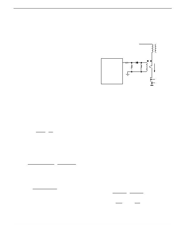
�Sensing� Current� with� a� Current� Sense� Transformer�
�At� higher� power� levels,� the� power� dissipation� in� a� current� sense�
�resistor� is� excessive.� A� current� sense� transformer� can� be�
�used� to� sense� the� current� while� minimizing� power� dissipation.�
�See� Figure� 11.� The� schematic� shows� the� circuitry� necessary�
�when� using� a� current� sense� transformer.� The� resistor,� R1,�
�provides� a� path� to� reset� the� current� sense� transformer.� The�
�resistor,� R2,� converts� the� scaled� down� current� to� a� voltage,�
�which� is� sent� to� the� ISNS� pin.�
�V� IN�
�V� ISNS� =� I� P� � R� ISENSE� +� I� ISNS� � R� f�
�where:� Ip� is� the� current� in� the� sense� resistor�
�R� ISENSE� is� the� current� sense� resistance�
�I� SNS�
�(pin� 14)�
�MIC9130�
�Rf�
�R2�
�R1�
�Current� Sense�
�Transformer�
�I� PRI�
�V� SENSE� 0.5�
�I� SENSE�
�R� SENSE� =� =� =� 0.5� Ω�
�V� ISNS� =� � R� 2� +� I� ISNS� � R� f�
�I� ISNS� is the current sourced from the ISNS pin�
�(40� μ� A)�
�R� f� is� the� series� resistor� between� the� ISNS� pin� and�
�the� current� sense� resistor.�
�The� current� sense� resistor� must� not� be� too� small� or� the� cur-�
�rent� sense� signal� will� be� susceptible� to� noise.� If� noise� is� a�
�problem,� the� current� signal� level� should� be� increased.�
�An� example� is� illustrated� below.�
�The� maximum� peak� current,� I� PMAX� =� 1A� at� 120%� overcurrent�
�and� minimum� input� voltage�
�The� maximum� rms� current,� I� RMS� =0.65A�
�The� desired� current� sense� signal� amplitude� is� 500mV� at� 1A�
�output� current.�
�The� current� sense� resistor� value� and� power� dissipation� is:�
�1�
�P� DISS� =� I� RMS� 2� � R� SENSE� =� 0� .� 65� 2� � 0� .� 5� =� 0� .� 21� W�
�A� 0.5� Ω� ,� non� inductive� resistor� with� at� least� a� 1/2W� rating�
�should� be� selected.�
�The� series� resistor� is� calculated� to� allow� the� 500mV-peak�
�signal� to� reach� 0.82V.�
�OUT�
�(pin� 16)�
�Figure� 11�
�The� voltage� at� the� ISNS� pin� is� calculated� by:�
�I� P�
�N�
�where:� I� P� is� the� current� in� the� primary� of� the� current� sense�
�transformer�
�R2� is� the� current� sense� resistance� at� the�
�secondary� of� the� current� sense� transformer�
�N� is� the� turns� ratio� of� the� current� sense�
�transformer� (N=Nsec/Npri)�
�I� ISNS� is� the� current� sourced� from� the� ISNS� pin�
�(40� μ� A)�
�R� f� is� the� series� resistor� between� the� ISNS� pin� and�
�the� current� sense� resistor.�
�Current� Transformer� example:�
�The� maximum� peak� current,� I� PMAX� =� 5A� at� 120%� overcur-�
�rent� and� minimum� input� voltage�
�V� ISNS� ?� (� I� P� � R� ISENSE� )� 0� .� 82� ?� (� 1� � 0� .� 5� )�
�I� ISNS�
�R� f� =�
�40μA�
�The� next� lower� value� of� 10k� Ω� is� selected.�
�=� 10� .� 25� k� Ω�
�The� maximum� rms� current,� I� RMS� =� 3.25A�
�The� full� 0.82V� peak� signal� a� the� ISNS� input� can� be� used�
�since� very� little� power� is� dissipation� in� the� secondary�
�side� sense� resistor.� The� maximum� peak� to� peak� volt-�
�The� bandwidth� of� the� 10K� resistor� and� the� 25pF� input� capaci-�
�tance� is� calculated.� The� resistor� value� must� be� lowered� if� the�
�bandwidth� is� too� low� for� the� switching� frequency.�
�age� at� the� sense� pin� (pin� 14)� is� 0.82V� at� the� 5A� maximum�
�output� current.�
�The� current� sense� resistor� value� and� power� dissipation�
�BW� =�
�=� 630� kHz�
�R� 2� =� SENSE�
�1�
�2� ×� π� ×� 10� k� ×� 25� pF�
�The� maximum� switching� frequency� of� this� power� supply�
�is:�
�V�
�I� P�
�� N�
�=�
�0. 82 × 100�
�5�
�=� 16� .� 4� Ω�
�?�
�?� I�
�?� 3� .� 25� ?�
�P� DISS� =� ?� PRMS� ?� � R� 2� =� ?� ?� � 16� .� 4� =� 17� .� 4� mW�
�should be approximately six times less than the BW to pre-�
�vent� current� waveform� distortion� and� excessive� delays� in�
�the� current� loop.� This� limits� the� switching� frequency� to� the�
�range� of� 100kHz.�
�2� 2�
�?� N� ?� ?� 100� ?�
�November� 2008�
�15�
�M9999-111108�
�相关PDF资料 |
PDF描述 |
|---|---|
| HSC25DRTI-S13 | CONN EDGECARD 50POS .100 EXTEND |
| EBC43DREI-S13 | CONN EDGECARD 86POS .100 EXTEND |
| ESM25DSAI | CONN EDGECARD 50POS R/A .156 SLD |
| ASM15DSAI | CONN EDGECARD 30POS R/A .156 SLD |
| RBC35DCMH | CONN EDGECARD 70POS .100 WW |
相关代理商/技术参数 |
参数描述 |
|---|---|
| MIC9131 | 制造商:MICREL 制造商全称:Micrel Semiconductor 功能描述:High-Voltage, High-Speed Telecom |
| MIC9131_06 | 制造商:MICREL 制造商全称:Micrel Semiconductor 功能描述:High-Voltage, High-Speed Telecom |
| MIC9131BM | 功能描述:IC CTRLR DC-DC PWM HV HS 16-SOIC RoHS:否 类别:集成电路 (IC) >> PMIC - 稳压器 - 专用型 系列:- 产品培训模块:Lead (SnPb) Finish for COTS Obsolescence Mitigation Program 标准包装:2,000 系列:- 应用:电源,ICERA E400,E450 输入电压:4.1 V ~ 5.5 V 输出数:10 输出电压:可编程 工作温度:-40°C ~ 85°C 安装类型:表面贴装 封装/外壳:42-WFBGA,WLCSP 供应商设备封装:42-WLP 包装:带卷 (TR) |
| MIC9131BM TR | 功能描述:IC CTRLR DC-DC PWM HV HS 16-SOIC RoHS:否 类别:集成电路 (IC) >> PMIC - 稳压器 - 专用型 系列:- 产品培训模块:Lead (SnPb) Finish for COTS Obsolescence Mitigation Program 标准包装:2,000 系列:- 应用:电源,ICERA E400,E450 输入电压:4.1 V ~ 5.5 V 输出数:10 输出电压:可编程 工作温度:-40°C ~ 85°C 安装类型:表面贴装 封装/外壳:42-WFBGA,WLCSP 供应商设备封装:42-WLP 包装:带卷 (TR) |
| MIC9131BQS | 功能描述:IC CTRLR DC-DC PWM HV HS 16-QSOP RoHS:否 类别:集成电路 (IC) >> PMIC - 稳压器 - 专用型 系列:- 产品培训模块:Lead (SnPb) Finish for COTS Obsolescence Mitigation Program 标准包装:2,000 系列:- 应用:电源,ICERA E400,E450 输入电压:4.1 V ~ 5.5 V 输出数:10 输出电压:可编程 工作温度:-40°C ~ 85°C 安装类型:表面贴装 封装/外壳:42-WFBGA,WLCSP 供应商设备封装:42-WLP 包装:带卷 (TR) |
发布紧急采购,3分钟左右您将得到回复。