- 您现在的位置:买卖IC网 > PDF目录18777 > MICRF001BN (Micrel Inc)IC RCVR/DATA DEMOD RF/IF 14DIP PDF资料下载
参数资料
| 型号: | MICRF001BN |
| 厂商: | Micrel Inc |
| 文件页数: | 6/8页 |
| 文件大小: | 0K |
| 描述: | IC RCVR/DATA DEMOD RF/IF 14DIP |
| 标准包装: | 25 |
| 频率: | 300MHz ~ 440MHz |
| 灵敏度: | -95dBm |
| 数据传输率 - 最大: | 4.8 kbps |
| 调制或协议: | OOK |
| 应用: | 车库门,RKE |
| 电流 - 接收: | 6.3mA |
| 数据接口: | PCB,表面贴装 |
| 天线连接器: | PCB,表面贴装 |
| 特点: | 自动调谐 |
| 电源电压: | 4.75 V ~ 5.5 V |
| 工作温度: | -40°C ~ 85°C |
| 封装/外壳: | 14-DIP(0.300",7.62mm) |
| 供应商设备封装: | 14-DIP |
| 包装: | 管件 |
�� �
�
�MICRF001�
�QwikRadio� tm�
�Micrel�
�External� Control� Signals� and� Mode� Selection�
�For� applications� where� the� transmit� frequency� is� accurately�
�set� for� other� reasons� (e.g.,� applications� where� a� SAW�
�transmitter� is� used� for� its� mechanical� stability),� the� user� may�
�choose� to� configure� the� MICRF001� as� a� standard�
�superheterodyne� receiver� (FIXED� mode),� mitigating� the�
�aforementioned� problem� of� a� competing� close-in� signal.� This�
�can� be� accomplished� by� tying� SWEN� to� ground.� Doing� so�
�forces� the� on-chip� LO� frequency� to� a� fixed� value.� In� such� a�
�case,� the� ceramic� resonator� would� be� replaced� with� a� crystal.�
�Generally,� however,� the� MICRF001� can� be� operated� with� a�
�ceramic� resonator� adequately,� no� matter� whether� the�
�transmitter� is� LC� or� SAW� based.�
�Slicing� Level� and� the� CTH� Capacitor�
�Extraction� of� the� DC� value� of� the� demodulated� signal� for�
�purposes� of� logic-level� data� slicing� is� accomplished� by�
�external� capacitor� CTH� and� the� on-chip� switched-cap�
�“resistor”� RSC,� indicated� in� the� block� diagram.� The� effective�
�resistance� of� RSC� varies� in� the� same� way� as� the�
�Demodulator� filter� bandwidth,� in� four� binary� steps,� from�
�approximately� 1600k� ?� to� 200k� ?� .� Once� the� filter� bandwidth�
�is� selected,� this� “resistance”� is� determined;� then� the� value� of�
�capacitor� CTH� is� easily� calculated,� once� the� slicing� level�
�time-constant� is� chosen.� Values� vary� somewhat� with�
�decoder� type,� but� typical� Slicing� Level� time� constants� range�
�5-50msec.� Optimization� of� the� CTH� value� is� required� to�
�maximize� range,� as� discussed� in� “Application� Note� 22,�
�MICRF001� Theory� of� Operation”,� section� 6.4.�
�AGC� Function� and� the� CAGC� Capacitor�
�The� signal� path� has� automatic� gain� control� (AGC)� to� increase�
�input� dynamic� range.� An� external� capacitor,� CAGC,� must� be�
�applied� to� set� the� AGC� attack� and� decay� time-constants.�
�With� the� addition� of� only� a� capacitor,� the� ratio� of� decay-to-�
�attack� time-constant� is� fixed� at� 10:1� (i.e.,� the� attack� time�
�constant� is� 1/10th� the� decay� time� constant),� and� this� ratio�
�cannot� be� changed� by� the� user.� However,� the� attack� time�
�constant� is� selectable� by� the� user� through� the� value� of�
�capacitor� CAGC.� By� adding� resistance� from� the� CAGC� pin�
�to� VDDBB� or� VSSBB� in� parallel� with� the� CAGC� capacitor,� the�
�ratio� of� decay-to-attack� time-constant� may� be� varied.� See�
�“Application� Note� 22,� MICRF001� Theory� of� Operation”.�
�Reference� Oscillator� (REFOSC)� and� External� Timing�
�Element�
�All� timing� and� tuning� operations� on� the� MICRF001� are�
�derived� from� the� REFOSC� function.� This� function� is� a� single-�
�pin� Colpitts-type� oscillator.� The� user� may� handle� this� pin� in�
�one� of� three� possible� ways:�
�(1)� connect� a� ceramic� resonator,� or�
�(2)� connect� a� crystal,� or�
�(3)� drive� this� pin� with� an� external� timing� signal.�
�The� third� approach� is� attractive� for� further� lowering� system�
�cost� if� an� accurate� reference� signal� exists� elsewhere� in� the�
�system� (e.g.,� a� reference� clock� from� a� crystal� or� ceramic�
�resonator-based� microprocessor),� and� flexibility� exists� in� the�
�choice� of� system� transmit� frequency.� An� externally� applied�
�signal� should� be� AC-coupled,� and� resistively-divided� down�
�(or� otherwise� limited)� to� approximately� 0.5Vpp.� The� specific�
�reference� frequency� required� is� related� to� the� system�
�transmit� frequency,� and� the� operating� mode� of� the� device� as�
�set� by� the� SWEN� control� pin.� See� “Application� Note� 22,�
�MICRF001� Theory� of� Operation”� for� a� discussion� of�
�frequency� selection� and� accuracy� requirements.�
�I/O� Pin� Interface� Circuitry�
�Interface� circuitry� for� the� various� I/O� pins� of� the� MICRF001� is�
�shown� in� Figures� 1� through� 6.� Specific� information� regarding�
�each� of� these� circuits� is� discussed� in� the� following� sub-�
�paragraphs.� Not� shown� are� ESD� protection� diodes� which�
�are� applied� to� all� input� pins.�
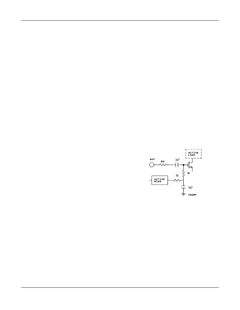
�1.� ANT� Pin�
�The� ANT� pin� is� internally� AC-coupled� via� a� 3pF� capacitor,� to�
�an� RF� N-channel� MOSFET,� as� shown� in� Figure� 1.�
�Impedance� on� this� pin� to� VSS� is� quite� high� at� low�
�frequencies,� and� decreases� as� frequency� increases.� In� the�
�UHF� frequency� range,� the� device� input� can� be� modeled� as�
�6.3k� ?� in� parallel� with� 2pF� (pin� capacitance)� shunt� to� VSSRF.�
�Figure� 1� ANT� Pin�
�2.� CTH� Pin�
�Figure� 2� illustrates� the� CTH� pin� interface� circuit.� CTH� pin� is�
�driven� from� a� P-channel� MOSFET� source-follower� biased�
�with� approximately� 20μA� of� bias� current.� Transmission� gates�
�TG1� and� TG2� isolate� the� 3.3pF� capacitor.� Internal� control�
�signals� PHI1/PHI2� are� related� in� a� manner� such� that� the�
�impedance� across� the� transmission� gates� looks� like� a�
�“resistance”.� The� DC� potential� on� the� CTH� pin� is�
�approximately� 2.2V,� fundamentally� determined� by� the� Vgs� of�
�the� two� P-channel� MOSFET� source-followers� shown.�
�June� 1998�
�6�
�MICRF001�
�相关PDF资料 |
PDF描述 |
|---|---|
| MICRF001BM TR | IC RCVR/DATA DEMOD RF/IF 14SOIC |
| AMB345906 | SENSOR REFL LONG V TYPE W/OSC |
| AMB345905 | SENSOR REFL LONG V TYPE W/OSC |
| AMB340912 | SENSOR REFL LONG H TYPE W/OSC |
| AMB340910 | SENSOR REFL LONG H TYPE W/OSC |
相关代理商/技术参数 |
参数描述 |
|---|---|
| MICRF001YM | 功能描述:射频接收器 300-440MHz RF Receiver( Lead Free) RoHS:否 制造商:Skyworks Solutions, Inc. 类型:GPS Receiver 封装 / 箱体:QFN-24 工作频率:4.092 MHz 工作电源电压:3.3 V 封装:Reel |
| MICRF001YM TR | 功能描述:射频接收器 300-440MHz RF Receiver( Lead Free) RoHS:否 制造商:Skyworks Solutions, Inc. 类型:GPS Receiver 封装 / 箱体:QFN-24 工作频率:4.092 MHz 工作电源电压:3.3 V 封装:Reel |
| MICRF001YM-TR | 功能描述:- RF Receiver OOK 300MHz ~ 440MHz -95dBm 4.8 kbps PCB, Surface Mount 14-SOIC 制造商:microchip technology 系列:- 包装:剪切带(CT) 零件状态:过期 频率:300MHz ~ 440MHz 灵敏度:-95dBm 数据速率(最大值):4.8 kbps 调制或协议:OOK 应用:车库门,RKE 电流 - 接收:6.3mA 数据接口:PCB,表面贴装 存储容量:- 天线连接器:PCB,表面贴装 特性:自动调谐 电压 - 电源:4.75 V ~ 5.5 V 工作温度:-40°C ~ 85°C 封装/外壳:14-SOIC(0.154",3.90mm 宽) 供应商器件封装:14-SOIC 标准包装:1 |
| MICRF001YN | 功能描述:射频接收器 300-440MHz RF Receiver ( Lead Free) RoHS:否 制造商:Skyworks Solutions, Inc. 类型:GPS Receiver 封装 / 箱体:QFN-24 工作频率:4.092 MHz 工作电源电压:3.3 V 封装:Reel |
| MICRF002 | 制造商:MICREL 制造商全称:Micrel Semiconductor 功能描述:300-440MHz QwikRadio? ASK Receiver |
发布紧急采购,3分钟左右您将得到回复。