- 您现在的位置:买卖IC网 > Datasheet目录55 > MICRF405YML TR (Micrel Inc)TRANSMITTER ASK/FSK 24-MLF Datasheet资料下载
参数资料
| 型号: | MICRF405YML TR |
| 厂商: | Micrel Inc |
| 文件页数: | 12/46页 |
| 文件大小: | 649K |
| 描述: | TRANSMITTER ASK/FSK 24-MLF |
| 标准包装: | 1 |
| 频率: | 290MHz ~ 980MHz |
| 应用: | ISM |
| 调制或协议: | ASK,FSK |
| 数据传输率 - 最大: | 200 kbps |
| 功率 - 输出: | 10dBm |
| 电流 - 传输: | 18mA |
| 数据接口: | PCB,表面贴装 |
| 天线连接器: | PCB,表面贴装 |
| 电源电压: | 2.2 V ~ 3.6 V |
| 工作温度: | -40°C ~ 125°C |
| 封装/外壳: | 24-VFQFN 裸露焊盘,24-MLF? |
| 包装: | 标准包装 |
| 产品目录页面: | 571 (CN2011-ZH PDF) |
| 其它名称: | 576-1965-6 |
第1页第2页第3页第4页第5页第6页第7页第8页第9页第10页第11页当前第12页第13页第14页第15页第16页第17页第18页第19页第20页第21页第22页第23页第24页第25页第26页第27页第28页第29页第30页第31页第32页第33页第34页第35页第36页第37页第38页第39页第40页第41页第42页第43页第44页第45页第46页
Micrel
MICRF405
April 2006
12
M9999-041906
(408) 955-1690
Writing to n Registers having Non-Incremental
Addresses
Registers with non-incremental addresses can be
written to in one write-sequence as well. Example of
non-incremental addresses:
0,1,3
. However, this
requires more overhead, and the user should
consider the possibility to make a
continuous
update, for example, by writing to
0,1,2,3
(writing
the present value of
2
into
2
). The simplest
firmware is achieved by always writing to all
registers. Refer to previous sections.
This write-sequence is divided into several sub-
parts:
" Disable the generation of load-signals by
clearing bit
load_en
(D0 in ControlRegister0)
" Repeat for each group of register having
incremental addresses:
- Bring SEN active
- Enter first address for this group, R/W bit and
values
- Bring SEN inactive
" Finally, enable and make a load-signal by
setting
load_en
Refer to the previous sections for how to write to 1 or
n (with incremental addresses) registers in the
MICRF405.
Reading from the Control Registers in MICRF405
The
read-sequence
is:
1. Enter address and R/W bit
2. Change direction of SIO line
3. Read out a number of octets and change SIO
direction back again.
It is possible to read all, 1 or n registers. The
address to read from (or the first address to read
from) can be any valid address (0-29). Reading is
not destructive, i.e., values are not changed. The
SIO line is output from the MICRF405 (input to user)
for a part of the read-sequence. Refer to procedure
description below.
A read-sequence is described for reading n
registers, where n is number 1-30.
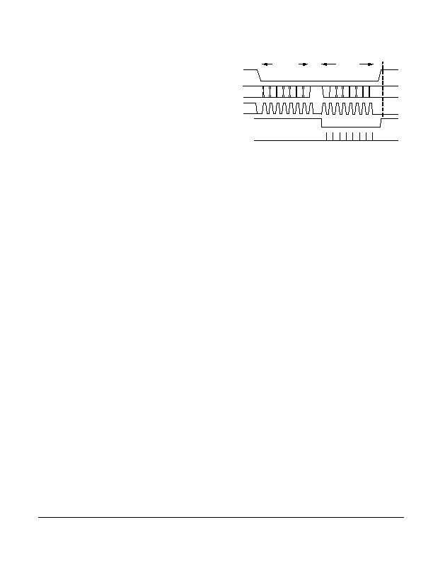
SEN
SIO
SCK
Register address
Data read
from register
Internal load pulse
generated here
A6A5A4A3A2A1A0R/W
D7D6D5D4D3D2D1 D0
SIO INPUT
SIO OUTPUT
SAMPLE TIME
Figure 4. Reading from a Control Register.
In Figure 4 above, 1 register is read. The address is
A6, A5, & A0. A6 = MSB. The data read out is D7,
D6, &D0. The value of the R/W bit is always
1
for
reading.
" Bring SEN low
" Enter address to read from (or the first address
to read from) (7 bits) and
" The R/W bit = 1 to enable reading
" Make the SIO line an input to the user (set pin in
tristate)
" Read n octets. The first rising edge of SLK will
set the SIO as an output from the MICRF405.
The 405 will change the SIO line at positive
edges of SCK. The user should read the SIO
line at the negative edges.
" Make the SIO line an output from the user again.
Reading from the Interrupt Register
If any of the interrupts, Vc_HI, Vc_LO or Low_Batt,
is set the SRV pin will go high. Read the interrupt
register, address 24, to see which interrupts are
flagged. It is possible to read this register at all
times, for instance, to read the tuned VCO_FREQ
setting which is also stored at the same address.
When rising SEN after haveing read the register, the
internal load pulse will then clear all interrupt flags.
To keep the flags when reading it, it is therefore
necessary to set LOAD_en=0 before hand.
相关PDF资料 |
PDF描述 |
|---|---|
| MTX-102-433DR-B | MODULE TRANSMITTER 433MHZ 18DIP |
| MTX-103-915DR-B | MODULE TRANSMITTER 915MHZ 18DIP |
| MTX-405-433DR-B | MODULE TRANSMITTER 433MHZ 24DIP |
| N50P105 | IC MODULE MINI JOYSTICK SMD |
| OCB350L187Z | BOARD CALIBR CIRCUIT OPB350L187 |
相关代理商/技术参数 |
参数描述 |
|---|---|
| MICRF500 | 制造商:MICREL 制造商全称:Micrel Semiconductor 功能描述:700MHz to 1.1GHz RadioWire RF Transceiver |
| MICRF500BLQ | 制造商:MICREL 制造商全称:Micrel Semiconductor 功能描述:700MHz to 1.1GHz RadioWire RF Transceiver |
| MICRF500BLQ TR | 功能描述:射频接收器 700-1000MHz, 3.0V, FSK, FH Transceiver RoHS:否 制造商:Skyworks Solutions, Inc. 类型:GPS Receiver 封装 / 箱体:QFN-24 工作频率:4.092 MHz 工作电源电压:3.3 V 封装:Reel |
| MICRF500BLQTR | 功能描述:TXRX UHF 700-1100MHZ 44-LQFP RoHS:否 类别:RF/IF 和 RFID >> RF 收发器 系列:- 产品培训模块:Lead (SnPb) Finish for COTS Obsolescence Mitigation Program 标准包装:30 系列:- 频率:4.9GHz ~ 5.9GHz 数据传输率 - 最大:54Mbps 调制或协议:* 应用:* 功率 - 输出:-3dBm 灵敏度:- 电源电压:2.7 V ~ 3.6 V 电流 - 接收:* 电流 - 传输:* 数据接口:PCB,表面贴装 存储容量:- 天线连接器:PCB,表面贴装 工作温度:-25°C ~ 85°C 封装/外壳:68-TQFN 裸露焊盘 包装:管件 |
| MICRF500EVAL1 | 功能描述:射频开发工具 MICRF500 Evaluation Kit - For experimental use only RoHS:否 制造商:Taiyo Yuden 产品:Wireless Modules 类型:Wireless Audio 工具用于评估:WYSAAVDX7 频率: 工作电源电压:3.4 V to 5.5 V |
发布紧急采购,3分钟左右您将得到回复。