- 您现在的位置:买卖IC网 > PDF目录371112 > MJ10009 (Boca Semiconductor Corp.) SWITCHMODE SERIES NPN SILICON POWER DARLINGTON TRANSISTORS WITH BASE-EMITTER SPEEDUP DIODE PDF资料下载
参数资料
| 型号: | MJ10009 |
| 厂商: | Boca Semiconductor Corp. |
| 英文描述: | SWITCHMODE SERIES NPN SILICON POWER DARLINGTON TRANSISTORS WITH BASE-EMITTER SPEEDUP DIODE |
| 中文描述: | 开关模式电源系列NPN硅达林顿晶体管的基射极加速比二极管 |
| 文件页数: | 6/8页 |
| 文件大小: | 235K |
| 代理商: | MJ10009 |
6
Motorola Bipolar Power Transistor Device Data
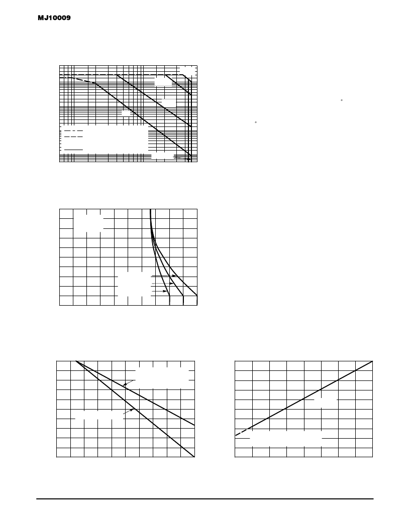
The Safe Operating Area figures shown in Figures 11 and 12 are
specified ratings for these devices under the test conditions
shown.
50
20
10
Figure 11. Forward Bias Safe Operating Area
VCE, COLLECTOR–EMITTER VOLTAGE (VOLTS)
5
1
0.5
0.1
0.05
0.005
6
10
20
600
BONDING WIRE LIMIT
THERMAL LIMIT @ TC = 25
°
C
(SINGLE PULSE)
SECOND BREAKDOWN LIMIT
50
I
dc
0.2
100
200
450
100
μ
s
10
μ
s
20
0
Figure 12. Reverse Bias Switching
Safe Operating Area (MJ10009)
VCE, COLLECTOR–EMITTER VOLTAGE (VOLTS)
16
12
0
500
4
I
8
300
400
100
200
VBE(off) = 5 V
VBE(off) = 2 V
VBE(off) = 0 V
1 ms
MJ10009
TC = 100
°
C
IC/IB1
≥
20
2
0.02
0.01
500
18
14
10
6
2
SAFE OPERATING AREA INFORMATION
FORWARD BIAS
There are two limitations on the power handling ability of a
transistor: average junction temperature and second break-
down. Safe operating area curves indicate IC – VCE limits of
the transistor that must be observed for reliable operation,
i.e., the transistor must not be subjected to greater dissipa-
tion than the curves indicate.
The data of Figure 11 is based on TC = 25 C; TJ(pk) is
variable depending on power level. Second breakdown pulse
limits are valid for duty cycles to 10% but must be derated
when TC
≥
25 C. Second breakdown limitations do not der-
ate the same as thermal limitations. Allowable current at the
voltages shown on Figure 11 may be found at any case tem-
perature by using the appropriate curve on Figure 13.
TJ(pk) may be calculated from the data in Figure 10. At
high case temperatures, thermal limitations will reduce the
power that can be handled to values less than the limitations
imposed by second breakdown.
REVERSE BIAS
For inductive loads, high voltage and high current must be
sustained simultaneously during turn–off, in most cases, with
the base to emitter junction reverse biased. Under these
conditions the collector voltage must be held to a safe level
at or below a specific value of collector current. This can be
accomplished by several means such as active clamping,
RC snubbing, load line shaping, etc. The safe level for these
devices is specified as VCEX(sus) at a given collector current
and represents a voltage–current condition that can be sus-
tained during reverse biased turn–off. This rating is verified
under clamped conditions so that the device is never sub-
jected to an avalanche mode. Figure 12 gives the complete
reverse bias safe operating area characteristics. See Table 1
for circuit conditions.
10
0
Figure 13. Power Derating
VBE(off), REVERSE BASE CURRENT (VOLTS)
7
5
0
2
5
8
7
2
I
IC = 10 A
1
SEE TABLE 1 FOR CONDITIONS,
FIGURE 7 FOR WAVESHAPE.
100
80
60
20
0
0
40
80
120
200
Figure 14. Reverse Base Current versus
VBE(off) with No External Base Resistance
TC, CASE TEMPERATURE (
°
C)
P
THERMAL DERATING
FORWARD BIAS
SECOND BREAKDOWN
DERATING
160
40
相关PDF资料 |
PDF描述 |
|---|---|
| MJ10009 | RADIATION HARDENED HIGH EFFICIENCY, 5 AMP SWITCHING REGULATORS |
| MJ10009 | NPN SILICON POWER DARLINGTON TRANSISTORS |
| MJ10009 | POWER TRANSISTORS(20A,400-500V,175W) |
| MJ1000 | Medium-Power Complementary Silicon Transistors |
| MJ1001 | Medium-Power Complementary Silicon Transistors |
相关代理商/技术参数 |
参数描述 |
|---|---|
| MJ10009 | 制造商:NTE Electronics 功能描述:T-NPN SI- PO DARL SW |
| MJ1000F | 制造商:Ohmite Mfg Co 功能描述: |
| MJ1000FE | 制造商:Ohmite Mfg Co 功能描述:Resistor;Metal Film;Res 100 Ohms;Pwr-Rtg 0.125 W;Tol 1%;Axial;Epoxy |
| MJ1000FE-R52 | 制造商:Ohmite Mfg Co 功能描述:Metal Film Resistors 1/8W 100 Ohm 1% 200 Volt |
| MJ1001 | 制造商: 功能描述: 制造商:Motorola Inc 功能描述: 制造商:undefined 功能描述: |
发布紧急采购,3分钟左右您将得到回复。