- 您现在的位置:买卖IC网 > PDF目录379321 > MJE18008 (ON SEMICONDUCTOR) POWER TRANSISTOR PDF资料下载
参数资料
| 型号: | MJE18008 |
| 厂商: | ON SEMICONDUCTOR |
| 元件分类: | 功率晶体管 |
| 英文描述: | POWER TRANSISTOR |
| 中文描述: | 8 A, 450 V, NPN, Si, POWER TRANSISTOR, TO-220AB |
| 封装: | CASE 221A-09, 3 PIN |
| 文件页数: | 5/10页 |
| 文件大小: | 421K |
| 代理商: | MJE18008 |
5
Motorola Bipolar Power Transistor Device Data
I
VCE, COLLECTOR–EMITTER VOLTAGE (VOLTS)
hFE, FORCED GAIN
TC
3
160
hFE, FORCED GAIN
Figure 13. Inductive Fall Time
tf
Figure 14. Inductive Crossover Time
I
Figure 15. Forward Bias Safe Operating Area
Figure 16. Reverse Bias Switching Safe
Operating Area
Figure 17. Forward Bias Power Derating
60
5
15
400
200
50
100
10
VCE, COLLECTOR–EMITTER VOLTAGE (VOLTS)
9
6
0
0
200
1,0
0,8
0,2
0,0
20
TC, CASE TEMPERATURE (
°
C)
80
140
160
1
0.01
3
600
1000
4
100
1000
DC (MJE18008)
5 ms
P
0,6
0,4
6
7
8
9
10
11
12
13
14
70
80
140
3
5
15
4
6
7
8
9
10
11
12
13
14
300
100
IC = 2 A
IC = 4.5 A
TJ = 25
°
C
TJ = 125
°
C
10
0.1
EXTENDED
SOA
1 ms
10
μ
s
1
μ
s
400
2
1
4
5
40
60
100
120
SECOND BREAKDOWN
DERATING
DC (MJF18008)
100
120
350
7
8
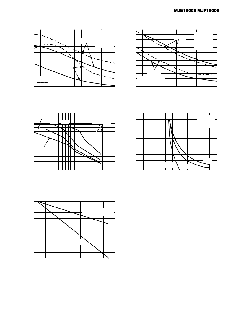
There are two limitations on the power handling ability of a
transistor: average junction temperature and second break-
down. Safe operating area curves indicate IC– VCE limits of
the transistor that must be observed for reliable operation;
i.e., the transistor must not be subjected to greater dissipation
than the curves indicate. The data of Figure 15 is based on TC
= 25
°
C; TJ(pk) is variable depending on power level. Second
breakdown pulse limits are valid for duty cycles to 10% but
must be derated when TC > 25
°
C. Second breakdown
limitations do not derate the same as thermal limitations.
Allowable current at the voltages shown in Figure 15 may be
found at any case temperature by using the appropriate curve
on Figure 17. TJ(pk) may be calculated from the data in Figure
20 and 21. At any case temperatures, thermal limitations will
reduce the power that can be handled to values less than the
limitations imposed by second breakdown. For inductive
loads, high voltage and current must be sustained simulta-
neously during turn–off with the base–to–emitter junction
reverse–biased. The safe level is specified as a reverse–
biased safe operating area (Figure 16). This rating is verified
under clamped conditions so that the device is never
subjected to an avalanche mode.
IB(off) = IC/2
VCC = 15 V
VZ = 300 V
LC = 200
μ
H
150
130
110
90
150
250
800
IB(off) = IC/2
VCC = 15 V
VZ = 300 V
LC = 200
μ
H
IC = 2 A
IC = 4.5 A
–1, 5 V
– 5 V
TC
≤
125
°
C
IC/IB
≥
4
LC = 500
μ
H
GUARANTEED SAFE OPERATING AREA INFORMATION
TYPICAL SWITCHING CHARACTERISTICS
(IB2 = IC/2 for all switching)
TJ = 25
°
C
TJ = 125
°
C
THERMAL DERATING
VBE(off) = 0 V
相关PDF资料 |
PDF描述 |
|---|---|
| MJE18008 | POWER TRANSISTOR 8.0 AMPERES 1000 VOLTS 45 and 125 WATTS |
| MJF18009 | POWER TRANSISTORS 10 AMPERES 1000 VOLTS 50 and 150 WATTS |
| MJF18009 | POWER TRANSISTORS |
| MJE18009 | POWER TRANSISTORS |
| MJE18009 | POWER TRANSISTORS 10 AMPERES 1000 VOLTS 50 and 150 WATTS |
相关代理商/技术参数 |
参数描述 |
|---|---|
| MJE18008G | 功能描述:两极晶体管 - BJT 8A 450V 125W NPN RoHS:否 制造商:STMicroelectronics 配置: 晶体管极性:PNP 集电极—基极电压 VCBO: 集电极—发射极最大电压 VCEO:- 40 V 发射极 - 基极电压 VEBO:- 6 V 集电极—射极饱和电压: 最大直流电集电极电流: 增益带宽产品fT: 直流集电极/Base Gain hfe Min:100 A 最大工作温度: 安装风格:SMD/SMT 封装 / 箱体:PowerFLAT 2 x 2 |
| MJE18009 | 制造商:ONSEMI 制造商全称:ON Semiconductor 功能描述:POWER TRANSISTORS |
| MJE180G | 功能描述:两极晶体管 - BJT 3A 40V 12.5W NPN RoHS:否 制造商:STMicroelectronics 配置: 晶体管极性:PNP 集电极—基极电压 VCBO: 集电极—发射极最大电压 VCEO:- 40 V 发射极 - 基极电压 VEBO:- 6 V 集电极—射极饱和电压: 最大直流电集电极电流: 增益带宽产品fT: 直流集电极/Base Gain hfe Min:100 A 最大工作温度: 安装风格:SMD/SMT 封装 / 箱体:PowerFLAT 2 x 2 |
| MJE180PWD | 功能描述:TRANSISTOR NPN 40V 3A RoHS:是 类别:分离式半导体产品 >> 晶体管(BJT) - 单路 系列:- 标准包装:1 系列:- 晶体管类型:NPN 电流 - 集电极 (Ic)(最大):1A 电压 - 集电极发射极击穿(最大):30V Ib、Ic条件下的Vce饱和度(最大):200mV @ 100mA,1A 电流 - 集电极截止(最大):100nA 在某 Ic、Vce 时的最小直流电流增益 (hFE):300 @ 500mA,5V 功率 - 最大:710mW 频率 - 转换:100MHz 安装类型:表面贴装 封装/外壳:TO-236-3,SC-59,SOT-23-3 供应商设备封装:SOT-23-3(TO-236) 包装:Digi-Reel® 其它名称:MMBT489LT1GOSDKR |
| MJE180STU | 功能描述:两极晶体管 - BJT NPN Epitaxial Sil RoHS:否 制造商:STMicroelectronics 配置: 晶体管极性:PNP 集电极—基极电压 VCBO: 集电极—发射极最大电压 VCEO:- 40 V 发射极 - 基极电压 VEBO:- 6 V 集电极—射极饱和电压: 最大直流电集电极电流: 增益带宽产品fT: 直流集电极/Base Gain hfe Min:100 A 最大工作温度: 安装风格:SMD/SMT 封装 / 箱体:PowerFLAT 2 x 2 |
发布紧急采购,3分钟左右您将得到回复。